You are now subscribed
Your newsletter sign-up was successful
Want to add more newsletters?

Every Friday
GamesRadar+
Your weekly update on everything you could ever want to know about the games you already love, games we know you're going to love in the near future, and tales from the communities that surround them.

Every Thursday
GTA 6 O'clock
Our special GTA 6 newsletter, with breaking news, insider info, and rumor analysis from the award-winning GTA 6 O'clock experts.

Every Friday
Knowledge
From the creators of Edge: A weekly videogame industry newsletter with analysis from expert writers, guidance from professionals, and insight into what's on the horizon.

Every Thursday
The Setup
Hardware nerds unite, sign up to our free tech newsletter for a weekly digest of the hottest new tech, the latest gadgets on the test bench, and much more.

Every Wednesday
Switch 2 Spotlight
Sign up to our new Switch 2 newsletter, where we bring you the latest talking points on Nintendo's new console each week, bring you up to date on the news, and recommend what games to play.

Every Saturday
The Watchlist
Subscribe for a weekly digest of the movie and TV news that matters, direct to your inbox. From first-look trailers, interviews, reviews and explainers, we've got you covered.

Once a month
SFX
Get sneak previews, exclusive competitions and details of special events each month!
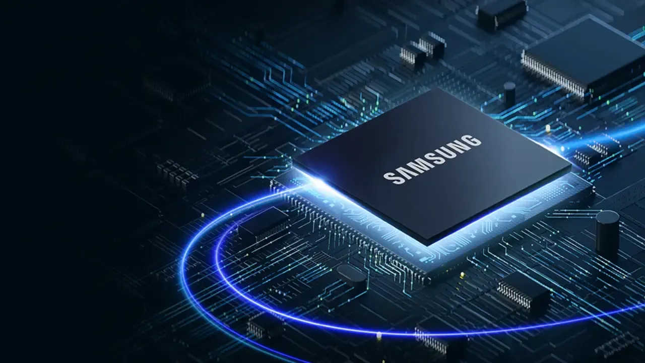
According to a new report on Korean outlet Dailian, Samsung has announced early results from mass production of its next-gen 2 nm chip node. But the company is only making very modest claims versus its existing 3 nm silicon.
Dailian quotes a Samsung report claiming, "the 2nm first-generation gate-all-around (GAA) process has improved performance by 5%, power efficiency by 8%, and area by 5% compared to the 3nm second-generation process." At first glance, those are not exactly mind blowing advances.

That said, consensus around the densities of the latest nodes generally puts Intel's 18A last on around 185 million transistors per square mm, Samsung SF2 next on about 200 million and TSMC's N2 out in front on 235 million.
Still, that at least makes Samsung SF2 broadly compatible with TSMC N2 for density. So, what about other measures? One of the most important is certainly yields, in other words the proportion of chips on a given wafer that actually work.
Such metrics are often closely guarded trade secrets. But according to the Dailian report, Samsung's yields for SF2 are in the 50% to 60% range, just high enough for commercial production. The same report puts TSMC's upcoming N2 node at 80%.
Normally, that would put Samsung at a clear disadvantage. But not necessarily this time. Yields matter mostly in terms of the impact they have on pricing. And TSMC is said to have put its wafer prices up dramatically in recent generations.
Indeed, the report says TSMC is planning to add another 10% to 20% to its pricing for N2. And that could create space for Samsung to undercut TSMC, even with inferior yields.
Samsung's SF2 is also its second to use GAA or Gate All Around technology. By contrast, TSMC's N2 node will be its first to offer GAA transistors, which improve performance, reduces power consumption and current leakage, and allow for smaller, more densely packed chips on a given node.
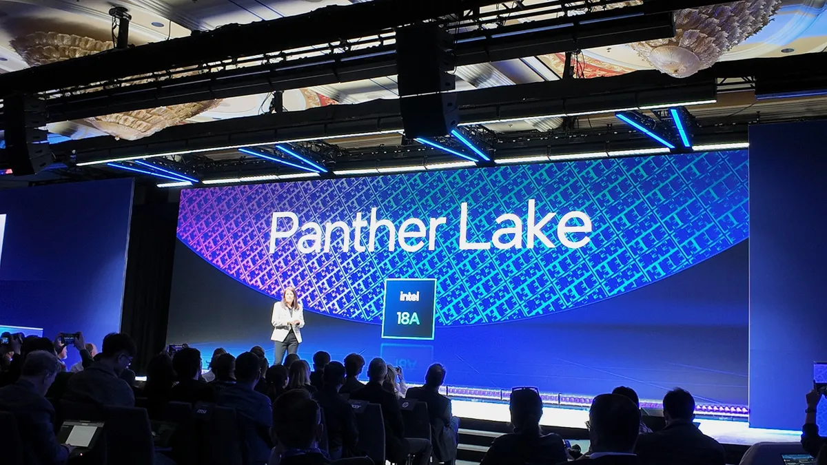
Ultimately, we'll have to wait for the first chip on these nodes to get a real feel for how they all compare. Intel's first 18A chip, Panther Lake, is due out in a few months at CES. TSMC's N2 node will likely first appear in an iPhone chip, probably in September.
As for Samsung's 2 nm tech, it's being used for a new Exynos 2600 smartphone chip designed for the upcoming Samsung Galaxy S26 handset. That's expected to launch early next year, meaning Samsung SF2 could beat TSMC N2 to market.
If that happens and Samsung's 2 nm tech looks healthy, it would be a very good thing for the chip market generally. Dailian says TSMC currently dominates the chip manufacturing industry, with 70.2% market share, nearly 10 times the 7.3% share of Samsung.
If Samsung could eat into that a bit, maybe the likes of AMD and Nvidia would have a realistic alternative for GPU production. And maybe graphics cards would get cheaper. Ha, OK, fat chance. But it's OK to hope, right?

Best graphics card 2025
All our current recommendations


You must confirm your public display name before commenting
Please logout and then login again, you will then be prompted to enter your display name.