Nanometer no more: Intel changes its process names to match TSMC
Promising to "innovate with the magic of silicon" Intel is pushing towards the sub-1nm 'angstrom era of semiconductors'.
Keep up to date with the most important stories and the best deals, as picked by the PC Gamer team.
You are now subscribed
Your newsletter sign-up was successful
Want to add more newsletters?
Intel is matching foundry rival, TSMC, node-for-node with its new process naming convention, but has also fired the first shot in the race for sub-nanometer terminology. Below 1nm, we're moving into what it's now calling the 'angstrom era of semiconductors'.
At the Intel Accelerated event CEO, Pat Gelsinger, has unveiled a detailed process roadmap for its future nodes, all tied into a new way to reference them. "We are accelerating our innovation roadmap to ensure we are on a clear path to process performance leadership by 2025," he says.
Gelsinger goes on to note that Intel "will be relentless in our pursuit of Moore’s Law and our path to innovate with the magic of silicon."
Article continues belowYou've got to love the way that Gelsinger is talking about his company now he's back and in the top job. I can't imagine Bob Swan or Brian Krzanich ever talking about 'the magic of silicon,' and it's refreshing to have some passion back in there with Intel's latest CEO.
This acceleration and re-marketing also reads as a smart move with Intel pushing forward with its IDM 2.0 strategy and launching its contract foundry business to rival the likes of TSMC. And what better way to measure yourself against the competition than by aligning your node naming conventions with theirs?
The industry has been talking about shifting the way it talks about process nodes for a while, with the nanometer terminology—once used to denote the gate length of a transistor—meaning less and less as time's gone on. From the moment transistors went three dimensional, with the move to FinFET (or Tri-Gate in Intel terminology) in 2011, a single dimension measurement has been rendered entirely irrelevant.
This has meant Intel increasingly looks behind the times. Through its manufacturing partner, TSMC, AMD has been able to show off nominally 7nm CPUs while Intel's desktop chips still languish on an old 14nm node.
Keep up to date with the most important stories and the best deals, as picked by the PC Gamer team.
But, as we've regularly pointed out here on PC Gamer, when it comes to transistor density, Intel's 10nm node is far more akin to TSMC's N7, or 7nm node.
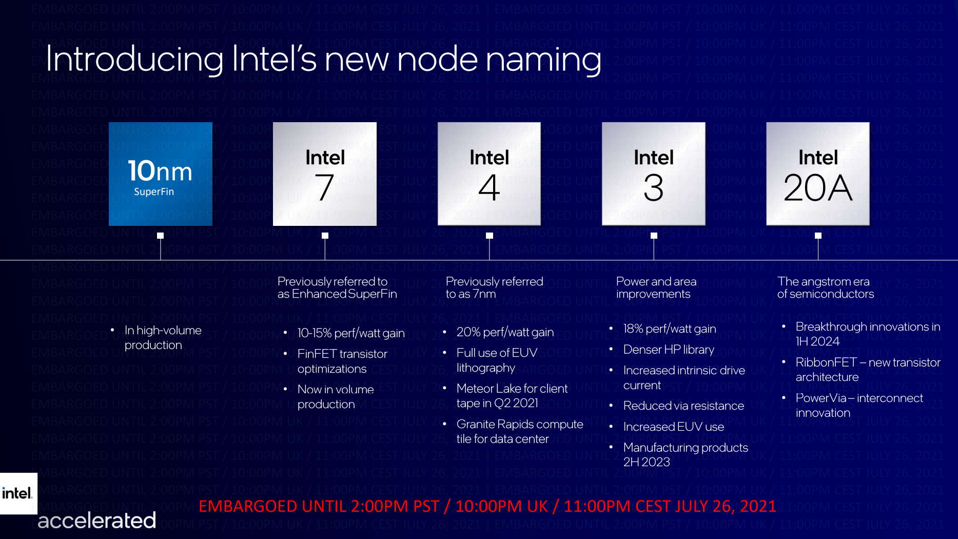
Which is why Intel is forgetting all that nanometer guff and, from the Enhanced SuperFin node forming the basis of the upcoming Alder Lake CPUs, will be using a new convention. First up will be 'Intel 7', which is the new name for the nominally 10nm Enhanced SuperFin node, and lines up against TSMC's N7 process.
Intel 7 is in volume production right now, and Intel claims giving it a new name is fair because of the 10 - 15% performance per watt gains this node is giving over the previous 10nm SuperFin. That's the sort of perf jump you'd expect from a new process, and Intel is now marketing it as such.
After that we hit 'Intel 4', which was previously referred to as 7nm and will line up against TSMC's N4 process, then we'll get 'Intel 3', and you can guess which rival node that's going head-to-head with.
Intel describes the advanced road map in a little more detail:
- Intel 7 delivers an approximately 10% to 15% performance-per-watt increase versus Intel 10nm SuperFin, based on FinFET transistor optimizations. Intel 7 will be featured in products such as Alder Lake for client in 2021 and Sapphire Rapids for the data center, which is expected to be in production in the first quarter of 2022.
- Intel 4 fully embraces EUV lithography to print incredibly small features using ultra-short wavelength light. With an approximately 20% performance-per-watt increase, along with area improvements, Intel 4 will be ready for production in the second half of 2022 for products shipping in 2023, including Meteor Lake for client and Granite Rapids for the data center.
- Intel 3 leverages further FinFET optimizations and increased EUV to deliver an approximately 18% performance-per-watt increase over Intel 4, along with additional area improvements. Intel 3 will be ready to begin manufacturing products in the second half of 2023.
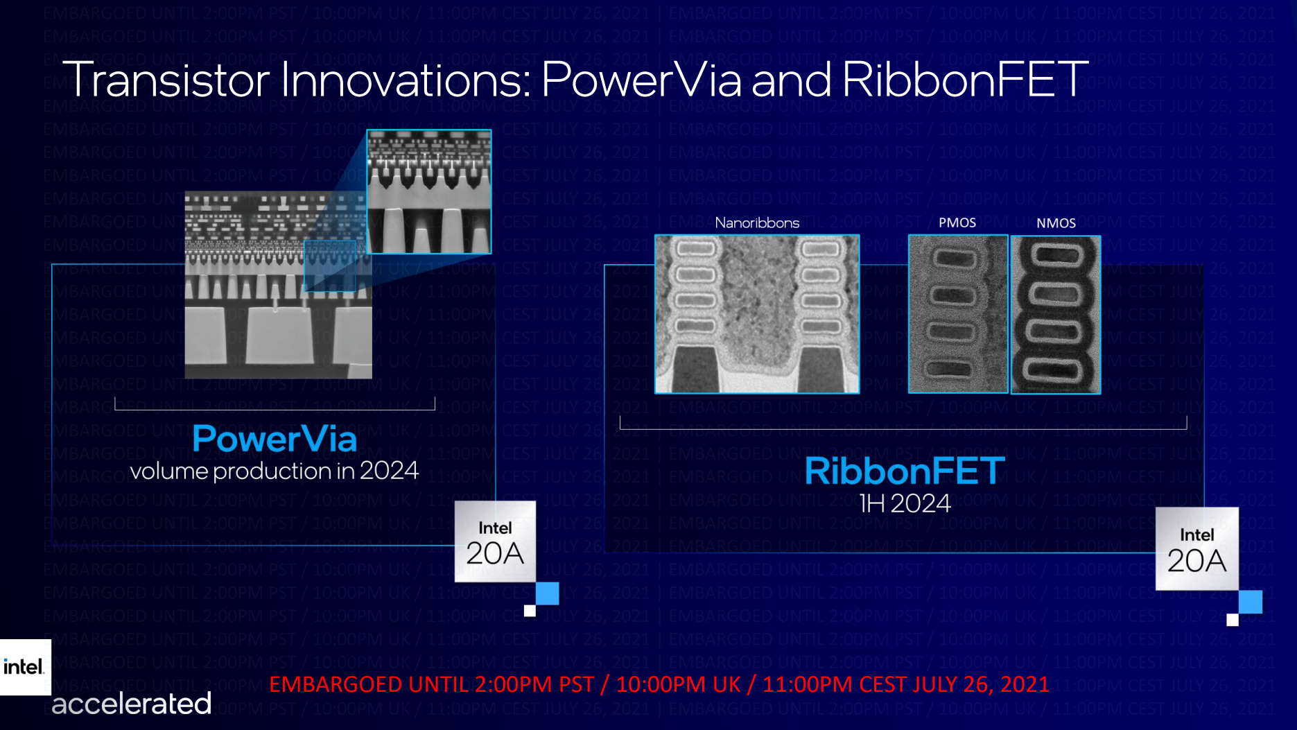
- Intel 20A ushers in the angstrom era with two breakthrough technologies, RibbonFET and PowerVia. RibbonFET, Intel’s implementation of a gate-all-around transistor, will be the company’s first new transistor architecture since it pioneered FinFET in 2011. The technology delivers faster transistor switching speeds while achieving the same drive current as multiple fins in a smaller footprint. PowerVia is Intel’s unique industry-first implementation of backside power delivery, optimizing signal transmission by eliminating the need for power routing on the front side of the wafer. Intel 20A is expected to ramp in 2024.
- 2025 and Beyond: Beyond Intel 20A, Intel 18A is already in development for early 2025 with refinements to RibbonFET that will deliver another major jump in transistor performance. Intel is also working to define, build and deploy next –generation High NA EUV, and expects to receive the first production tool in the industry. Intel is partnering closely with ASML to assure the success of this industry breakthrough beyond current generation of EUV.
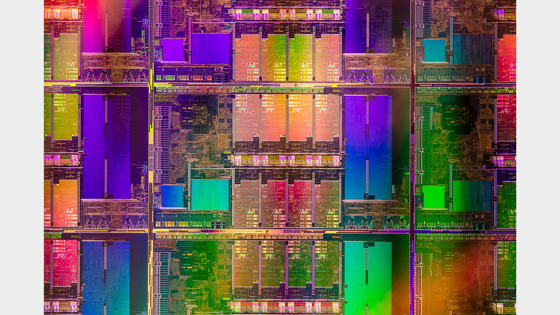
Admittedly, the whole idea is less for the likes of us and is more about marketing itself to potential customers for its fledgling foundry business. Though it will hopefully make it clearer where different process nodes line up against each other when we're talking about new chips from different manufacturers.
After that is where things get super-interesting though, as beyond the Intel 3 products shipping at the tail end of 2023, we then move into another wholly new naming convention. This is the industry moving towards a nominally sub-1nm era, with the name 'Intel 20A' being giving to its first new process node of the angstrom era of semiconductors in the first half of 2024.
Though this might be where Intel's simplified node naming convention gets complicated again. An angstrom is literally a sub-nanometer unit of measurement, with one angstrom equalling 0.1nm. But Intel is at pains to point out that, despite the 'A' in 'Intel 20A' standing for angstrom, it is purely a name, not a measurement. So, to be clear, Intel 20A is not a process incorporating transistors measuring 2nm in terms of their gate length.
These new angstrom era chips not only come with a new naming convention—that I'm sure Intel will hope catches on—but will also incorporate the first new Intel transistor design since that 22nm FinFET in 2011. RibbonFET, also known as NanoSheet, or Gate All Around (GAA), will land with Intel 20A in 2024. It's a transistor design that should speed up the switching (from 0s to 1s) as well as being able to cope with the power demands of modern CPUs in an ever smaller, more densely packed environment.
Intel 20A will also incorporate a new power delivery method, call PowerVia. That in itself will offer the three dimensional chips of tomorrow something called 'backside power delivery' optimising against leakage and for signal transmission by removing the need to have power routing on the front side of a given wafer.
This is all super techy manufacturing process style stuff, and a bit future gazing. But the short of it is that Intel is aiming to have process performance per watt leadership by the time its Intel 18A node rolls around in 2025. Though Intel reps are keen to point out that is a very different thing to having products with performance leadership—it's expecting to have those much sooner.

Dave has been gaming since the days of Zaxxon and Lady Bug on the Colecovision, and code books for the Commodore Vic 20 (Death Race 2000!). He built his first gaming PC at the tender age of 16, and finally finished bug-fixing the Cyrix-based system around a year later. When he dropped it out of the window. He first started writing for Official PlayStation Magazine and Xbox World many decades ago, then moved onto PC Format full-time, then PC Gamer, TechRadar, and T3 among others. Now he's back, writing about the nightmarish graphics card market, CPUs with more cores than sense, gaming laptops hotter than the sun, and SSDs more capacious than a Cybertruck.
