


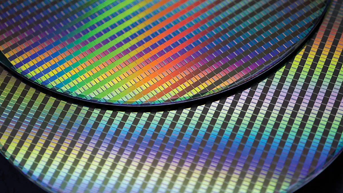
You'll likely have heard of the term "process node leadership" being bandied about from the red camp lately. It's a term AMD hasn't been able to use until recently with the advent of its Ryzen 3000 processors manufactured on the 7nm process node from TSMC. But behind the scenes there's an even greater debate raging on in chip making: what decides a process node's name, and what does it stand for?
In a recent paper, researchers suggest that semiconductor companies should ditch the loosely defined transistor gate length as a measure of technological advancement (i.e 7nm or 14nm), and instead focus on transistor density. That's near-enough the same metric Intel's been proposing for years now, but this time it's also tacitly supported by Intel's greatest rival, TSMC.
Well, one researcher from TSMC at the very least. The paper is titled "A Density Metric for Semiconductor Technology," and can be found in Proceedings of the IEEE, vol. 108, no. 4, pp. 478-482, April 2020 (via TechPowerUp). It's nine authors hail from Stanford, MIT, Berkeley, and TSMC. Within the team posit that a change is required to standardise the advances in semiconductor lithographic manufacturing technology across the industry.

It's a proposal to combat an age-old problem. You'll likely have heard of the terms 14nm, 12nm, 10nm, and 7nm thrown around a lot. That's because these are key technologies at the foundation of Intel, AMD, and Nvidia's chips. The smaller the better, right?
Well, not exactly. Despite the general trend towards smaller and smaller transistor lengths marking an improvement in power efficiency and performance, it's not always as straightforward as that. With many competing technologies and companies involved, and playing by their own rules as to how they define transistor length, the name attached to process node isn't so much a technical term as it is a marketing one.
"Driven by competitive marketing in the most recent decade," the researchers say, "this label has become decoupled from, and can be several times smaller than, the actual minimum gate length, while it also fails to convey other essential characteristics of the technology."
With power and performance disparities of up to 40% between nodes on the line, process node performance is a key metric in determining which chip ends up with the best CPU for gaming crown.
There's also the problem of what do we name chips once someone dips below 1nm? TSMC is already working on its 2nm process node, so we'll reach that point sooner than you might think. As far as semiconductors go, silicon still has some legs in it yet, so best find a new metric that represents that sharpish—it's also the perfect time to finally "clear up the node naming mess" as Intel once put it.
The research paper outlined over at IEEExplore defines a process of measuring semiconductor advancement by a different metric: density. It's a holistic approach, too. Rather than simply measure logic transistor length, the researchers propose a measure of logic, memory, and packaging/integration technologies simultaneously.
"Since its inception, the semiconductor industry has used a physical dimension (the minimum gate length of a transistor) as a means to gauge continuous technology advancement," the researchers say within the paper. "This metric is all but obsolete today. As a replacement, we propose a density metric, which aims to capture how advances in semiconductor device technologies enable system-level benefits."
It's called the Logic, Memory, Connectivity Metric, or LMC for short, and substitutes a single transistor length for a three-part number, consisting of DL, DM, and DC values. DL is the density of logic transistors, DM is the bit density of main memory (off-chip DRAM for the most part today), and DC is the density of connections between main memory and logic. All are measured in mm2.
If your system has lots of cores, memory, and bandwidth—a supercomputer, for example—it's going to come out on top with LMC.

That's the thing with LMC, it's more a system measurement formula than a straightforward measure of the lithographic processes that which we use today. It would also mean that our metric for a chip's worthiness is abstractly generated from system configuration, which is highly variable between machines and dependent on components such as system memory. The first measurement, DL, would serve as the more accurate analogue to the measures in use industry-wide today.
A singular transistor density metric, much like DL, has long been the metric that Intel would like to see the industry adopt. Intel's ex-director of process, Mark Bohr, posited a solution that would measure density of 2-input NAND cells and scan flip flop cells and spit out a single transistors/mm2 measurement. Since this approach doesn't account for SRAM cell size, which differs wildly on a chip-by-chip basis, Intel suggests including a separate measurement alongside logic density.
Intel is likely to be keen on adopting a new standard metric as it tends to come out on top in raw transistor density as it stands today. Intel reports a density of 100.76MTr/mm2 (mega-transistor per squared millimetre) for its 10nm process, while TSMC's 7nm process is said to land a little behind at 91.2MTr/mm2 (via Wikichip). Not that it'll do you much good on desktop—Intel's yet to produce 10nm desktop processors. AMD Ryzen on the other hand….
It will take a little convincing to shift an entire industry away from its "proof is in the pudding" approach and over to a universal density metric, but both the researchers and Intel agree that a density approach would prove universally more useful in measuring semiconductor progress. LMC's three metrics would also act as fine markers for the improvements on the way as a result of the many advanced packaging technologies in development, such as 3D stacking.
So here's hoping we see LMC, or something similar, for future process nodes. As the researchers eloquently put it, "the quandary of using the vanishing nanometre" is reaching critical mass, so we best get a move on implementing it too.