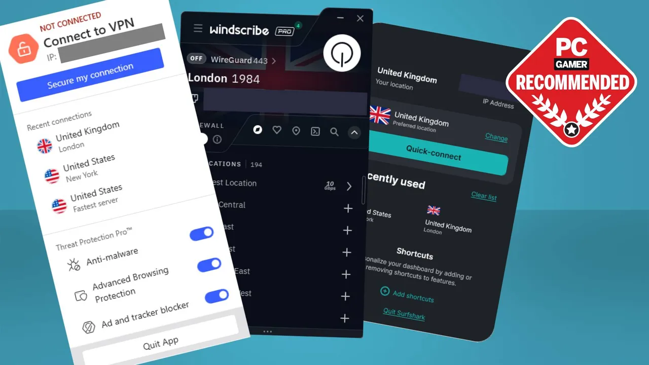
 Join The Club


Nvidia's new Hopper server GPU architecture has spawned a mammoth chip. And I'm not even talking about the 80 billion transistor H100 graphics processor itself. Nope, the new NVSwitch baked into the DGX 100 server system is reportedly home to some 25 billion transistors—that's just shy of the number inside the GA102 GPU inside the RTX 3090.
That 3rd gen NVLink switch chip of the Hopper generation is a monster of its own. It’s also manufactured at TSMC 4N and has 25 billion transistors. The switch offers 64 NVLink ports.The predecessor had 2 billion transistors, was manufactured in TSMC 12 nm and offered 18 ports. pic.twitter.com/37tG229HGsMarch 25, 2022
The NVSwitch chip is the interconnect which allows multiple instances of NVLink—the direct chip-to-chip connection—to talk and enable lots of Nvidia graphics cards to work together. That means they can pool their resources to power through complex calculations faster than a single GPU, or even two GPUs, would be able to on their own.
Think SLI, but connecting lots of chips and, y'know, effective.

This 3rd Gen version is built on the same TSMC 4N node as the H100 chip itself, and is able to directly connect up to eight GPUs with chip-to-chip bandwidth of 900GB/s and a total aggregate bandwidth of 7.2TB/s.
I'm only really referencing those numbers because they are so damned big, not because they have any bearing on us or PC gaming. The Hopper architecture is one designed purely for the server environment, and the NVSwitch interconnect doubly so.
Discrete GPUs didn't really game well together when SLI and CrossFire were actually a thing, and it's only in the more compute-centric environment that genuine multi-GPU processing exists. But even there you need seriously high-speed links to get the most out of these high-speed processors, and that's presumably why Nvidia has specced out the NVSwitch with so many damned 4nm transistors.

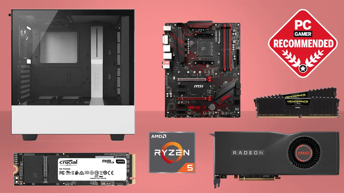
Best CPU for gaming: The top chips from Intel and AMD
Best gaming motherboard: The right boards
Best graphics card: Your perfect pixel-pusher awaits
Best SSD for gaming: Get into the game ahead of the rest
For reference, the GA102 GPU, the biggest chip in the GeForce sphere, comes in at 28.3 billion transistors—so a few billion more than the NVSwitch. On the AMD side, the Navi 21 GPU running the RX 6900 XT, 6800 XT, and RX 6800 is closer at 26.8 billion. But it's still considerably more than the 17.4 billion transistors of the GA104 chip which powers the RTX 3070 Ti, down to some RTX 3060 cards.
So yes, a big ol' chip.
But we're likely to see more big ol' chips coming in the next generation of graphics cards, and the red team is also going to bring back the idea of multi-GPU gaming, too. Not necessarily in the same way as CrossFire, however, think more like the chiplet design of its Ryzen processors and you'll be on the right track.
The key to multi-GPU gaming is for the OS to see it all as one single chip, and it looks like AMD has figured out an internal GPU interconnect that will do that, and enable its top Radeon RX 7000-series cards to sport a multi-chip design. And potentially out muscle the expected monolithic design of Nvidia's future Lovelace-based RTX 4000-series cards.