It's been recently put forward that AMD may be considering a multi-chip GPU for its upcoming graphics card generation, one which features two or more discrete chips intrinsically tied together to work as one for maximum performance. A truly massive 160 CU GPU, in fact. It's a concept not unlike the one that AMD employs within its AMD Ryzen CPUs, and with great success, but is it really possible in graphics?
This is hardly the first time we've heard tell of a multi-chip GPU, which is often referred to as an MCM GPU, for multi-chip module. Even way back in the days of Vega, and ahead of first generation RDNA, then known as Navi, AMD's key engineers and project leads were keen on the concept.
We are looking at the MCM type of approach, but we’ve yet to conclude that this is something that can be used for traditional gaming graphics type of application.
David Wang, SVP engineering AMD, 2018
Then-AMD employee and RTG lead Raja Koduri said that high-bandwidth interconnects, powered by Infinity Fabric, were key to pairing the company's IPs and that it "forms the basis of all of our future ASIC designs". He even specifically went to mention multi-GPU designs at the time, claiming it was indeed possible with Infinity Fabric.
That was back in 2017, and a lot has changed since. Not the least bit Raja Koduri leaving AMD to head up Intel's graphics department, among other things. Roadmaps are also likely to have shifted around some.
For the most part MCMs have seemed to remain in the concept stage ever since, but that's perhaps deceiving of the work behind the scenes into the many technologies required to bring such a GPU package together in reality.
We've recently seen the emergence of patents from AMD that just might allude to some of that work. First filed in June 2019, the primary patent called 'GPU chiplets using high bandwidth crosslinks' alludes to such an approach moving out of the theoretical and into the practical. At least signifying, in some way, that there's a chance in heck that such an MCM design could see an uplift in gaming performance for future GPU generations.
Now there's a key distinction to make between a MCM GPU and a graphics card with multiple GPUs on it. An MCM GPU is a single discrete package, which isn't the same as, say, the Radeon HD 5790, which employed all the necessary components of a single graphics card but twice over. The latter makes for a very stuffy PCB, and requires some form of frame sharing process like any other gaming PC with multiple graphics cards today: an onboard bridge replacing what would otherwise be a Crossfire or SLI bridge between two discrete cards.

So why complicate things further? For one, multiple graphics cards working in tandem requires a lot external support, hence why they're now toast for the most part in gaming. But there's another reason why AMD will be eyeing up a MCM approach: even the existing GPU dies from AMD and rival Nvidia are pushing the limits of existing manufacturing processes. They're some of the single largest dies in production, well, ever.
AMD's top GPU today is Navi 21, found within both RX 6800-series GPUs and the RX 6900 XT. At 519mm2, it's a significantly large chip. Nvidia's RTX 3090 GA102 GPU is 628mm2.
Both are verging on the maximum reticle field size of existing lithographic machines, often called the reticle limit. Dutch company ASML is the world leader in lithographic tools today, and its sub-20nm tools, capable of a numerical aperture (NA) of 1.35, can deliver a maximum field size of 858mm2. That's the largest die size, effectively, for any chip to be manufactured on that machine with a single mask. In reality, even producing something of that scale would be difficult, costly, and likely not up to preferable yields.
Which is all to say neither AMD or its competitors are able to simply crack a whole bunch more cores on a single chip and call it a day—even without considering packaging, PCBs, or power.
So naturally there's some urgency in AMD's quest for alternatives. Chiplets are one such option. With much smaller footprints, more dies can be made per wafer, there's greater flexibility with the end product, and there are options if you want to increase overall performance drastically. Most of all, chiplets help reduce cost.
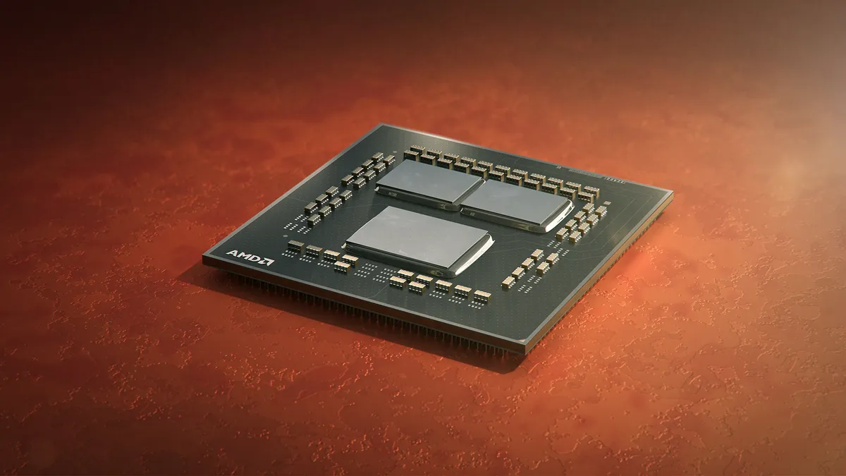
Of course, that's something AMD has some experience with its AMD Ryzen CPUs. Since the introduction of Zen 2, AMD has delivered chiplets containing the CPU cores packaged alongside a I/O die, all of which communicates together with fairly low latency, all things considered. Those 7nm chiplets containing the Zen cores, AMD says, cost half as much to manufacture as a an equivalent 7nm chip would of the same core count. So you can already see what's in it for AMD, and us customers get to play around with 16-core desktop chips.
But even chiplets throw up whole other hurdles that must be overcome in order to get them working. While AMD's done so in the CPU, the GPU is not such a simple beast.
Back in 2018, David Wang, senior vice president of engineering at AMD (RTG), touched a little on why an MCM GPU isn't all that easy to put together in a chat documented by our very own Dave James while at PCGamesN.
“We are looking at the MCM type of approach,” says Wang, “but we’ve yet to conclude that this is something that can be used for traditional gaming graphics type of application.
“To some extent you’re talking about doing CrossFire on a single package. The challenge is that unless we make it invisible to the ISVs [independent software vendors] you’re going to see the same sort of reluctance.
“We’re going down that path on the CPU side," Wang continues, "and I think on the GPU we’re always looking at new ideas. But the GPU has unique constraints with this type of NUMA [non-uniform memory access] architecture, and how you combine features… The multithreaded CPU is a bit easier to scale the workload. The NUMA is part of the OS support so it’s much easier to handle this multi-die thing relative to the graphics type of workload.”
Don't give up hope just yet. That's not a death sentence for MCM GPUs, as Wang was keen to mention even back then. "Anything's possible… " he concludes. It just poses even more hurdles that need to be surmounted before a multi-chip GPU can make it to market.
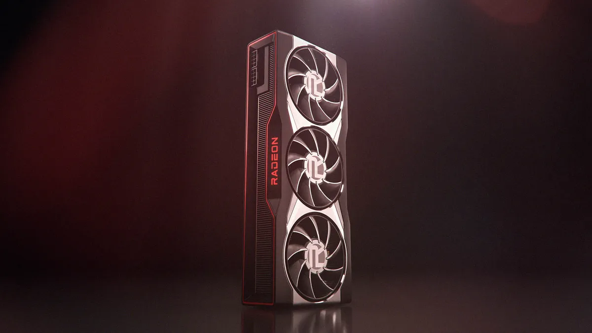
The basis for future gaming GPUs lies with the RDNA architecture. That's now in its second iteration, RDNA 2, which serves up impressive performance with some clever innovations. Infinity Cache is the architecture's headline feature, but heaps of optimisations have been made to get the second-gen gaming cards significantly faster for gaming than the first.
There are certain breakthroughs in packaging and interconnects that needed to exist prior to an earnest attempt to make a MCM GPU design—but it's just as much a question of software, too. It's not easy to have two discrete GPUs, however closely linked, act together as one, or be seen as one by a range of systems. PCs aren't known for their uniformity, either.
It needs to be able to do so with such a degree of ease and simplicity that the separate components of an MCM will be able to act as one for the purpose of parallel processing—a GPU's bread and butter. Splitting out sections of a GPU pipeline across chiplets, and with varying memory access between them, requires ever-increasing complexity in designs.
Like I mentioned with Crossfire and SLI, this has historically required a lot of tinkering by devs on the software side, and frankly no one can be bothered to do so for what little return there is given how few gamers actually run multi-GPU setups. But unlike multiple graphics cards, or even multi-GPU graphics card, a multi-chip GPU may be able to trick the system into thinking its constituent parts are one and the same, as the interconnects are that much closer to the metal.
That's the thinking, anyways, and most recently expectations of such a chip from AMD have been bolstered by the arrival of fresh patents from the filing cabinet. Well, fresh in a sense. The primary patent regarding this, that one specifically on GPU chiplets across high bandwidth crosslinks, was originally filed in June 2019. You can bet your bottom dollar AMD was working on it long before that, though.

Credited to Skyler Saleh, Sam Naffziger, Milind Bhagavat, and Rahul Agarwal, the patent explains how an array of GPU chiplets may be coupled to a second GPU chiplet through the use of 'passive crosslink'. This passive crosslink is an interposer die that's dedicated to communication between chiplets, or system-on-chip functions in some cases.
The reasons for such an approach, AMD explains, are pretty clear. Monolithic dies are expensive and yields could be better. To get around that, and importantly improve system performance, AMD hopes to create a multi-chip GPU that can operate with the existing programming model.
You hear that? That's ISVs everywhere breathing a sigh of relief.
What's important in such a design is cache coherency. Even if you shift the cache onto another chiplet, its access is seemingly uniform for a CPU.
Here's an excerpt from the patent filing that goes into the exact process:
"During operations, a memory address request from the CPU to the GPU is transmitted only to a single GPU chiplet, which then communicates with a high bandwidth passive crosslink to locate the requested data. From the CPU's point of view, it appears to be addressing a single die, monolithic GPU. This allows for use of a large-capacity, multi-chiplet GPU that appears as a single device to an application."
To the CPU, the GPU may as well be monolithic. It is none the wiser. And that means the software need not need be any wiser either.
Yet there's still the issue of latency. How long it takes for that request to be carried out by the GPU, especially if it's going from one extreme of one chip to another. That's where, it would appear, bandwidth plays a pivotal role. Those crosslink connections will need to be able to keep up with a constant back and fourth of data that a massively-parallel GPU will require in order to operate to offer worthwhile performance.
But that's not the only patent related to chiplets from AMD. Here's one for a cache and machine learning accelerator chiplet. Or this one for a crosslink die. You look through AMD's recent patents and you'll find many patents that could be useful for a chiplet architecture, whether in regards to a GPU or CPU.
Yet patents aren't a guarantee of intention, and major tech companies like Intel, AMD, and Nvidia register patents daily. In fact, Nvidia has published research papers and worked on prototype multi-die AI processors in the past, none of which have led to its adoption of multi-GPU chips. So far…
“This gives us a bunch of technologies on the shelf that at some point in time,” Nvidia's chief scientist, Bill Dally, said of multi-chip GPUs, “if it became economically the right thing to do to, assemble GPUs from multiple chiplets, we basically have de-risked the technology. Now it’s a tool in the toolbox for a GPU designer.”
So perhaps you'll see something similar out of Nvidia in good time.
It appears as though Intel may skip the high-performance monolithic dies altogether with Intel Xe, too. The company's maiden voyage (for the most part) into GPUs is leading it right down the path of heterogenous GPU dies made up of chiplets, or what Intel would rather call 'Tiles'.
But is an AMD MCM GPU possible in the near-future? To put it plainly, yes. Would such a card necessarily land in our gaming machines? That, sadly, we can't say for sure.
The rumour mill is expectantly waiting for the arrival of a multi-chip GPU as soon as Navi 31—yeah, as soon as the next-gen RDNA 3 architecture arrives. But that's far from a guarantee, even born out of some prolific Twitter leakers as it is.

My initial hesitancy comes from the fact we're yet to see a CDNA multi-chip GPU. AMD forked its graphics architectures into RDNA and CDNA fairly recently—the former being for gaming and the latter being for compute. Such as it is that you'll find RDNA in the RX 6000-series and CDNA in the Instinct MI100.
The Instinct MI100 is an absolute beast of a GPU. AMD tore just about everything you'd need to game on this card off the silicon and stuffed the spaces with even more compute units, for a total of 120. That's 50% more than 'Big Navi'. That dramatically increases the computational might of this card, which makes it fit to operate at pace in its primary function: chomping down on numbers in a data centre.
Datacentres are geared towards raw bandwidth and raw compute, and it's in these settings that a card with as much of both as you can get. A multi-chip GPU seems a perfect fit, no?
AMD has as much reason, if not more, to first get a multi-chip GPU working for the datacentre ahead of any gaming aspirations of a similar ilk. A far more controlled ecosystem than PCs as a whole, and with a focus on raw compute over frame-by-frame speed, it appears the easier first step into a world of cross-chip communication in graphics, too—it's where Intel's placing its first tile-based GPU, Ponte Vecchio.
There are sure to be further considerations, however, and gaming is a significantly larger market for AMD's GPUs than its server accelerators. Such a CDNA GPU could well be in the works, too.
And I'm just about willing to look past any initial apprehension for the slim hope of gaming on the feigned RDNA 3 160 CU behemoth that everyone's longing for. That's said to be comprised of two 80 CU chiplets—a total of 10,240 cores in total. A chip that would make such a mockery of the so-called 'Big Navi' that we'll have to retroactively rename the RX 6900 XT to something more more befitting its slender CU count.
I don't dare consider the TDP of such a monster—the 80 CU AMD RX 6900 XT comes in at 300W alone.
The introduction of chiplets with the Zen 2 architecture has been so incredibly beneficial to the AMD's CPU division that getting said engineering smarts over to the GPU side pronto seems a given. We know AMD's keen to share what it's learned with Zen on the graphics side—an approach that's paid dividends with RDNA 2, the 7nm process, clock speeds, and cache—and chiplets would make for a clever cooperative venture, that's for sure.
Whichever way you slice it, MCM GPUs are the likely answer to growing monolithic chip costs and limitations.