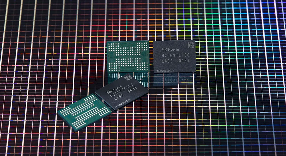
SK Hynix has developed what it is calling the "industry's most multi-layered" 176-layer 4D NAND flash memory, currently offered in 512 gigabit (64GB), triple-level cell (TLC) form. The move to a 176-layer design promises more capacious storage products, including SSDs, with faster speeds to boot.
The numbers kind of jump around all over the place, but SK Hynix says the shift to 176-layer NAND increases bit productivity by 35 percent compared to the previous generation (96-layer), while pushing 20 percent faster read speeds of individual cells, and 33 percent faster data transfer speeds.

Best CPU for gaming: the top chips from Intel and AMD
Best graphics card: your perfect pixel-pusher awaits
Best SSD for gaming: get into the game ahead of the rest
How all that translates to the performance of actual shipping products remains to be seen. To that end, however, SK Hynix alludes to mobile products being the first recipients for 176-layer NAND, with 70 percent faster maximum read speeds and 35 percent faster writes. Those will arrive by the middle of next year, followed by both consumer and enterprise SSD products.
Today's NAND flash memory products already utilize a stacked design, hence the 3D designation. But memory makers have taken things about as far as they can go, utilizing floating gates and traditional cell structures. In contrast, 176-layer designs make use of a technology called charge trap flash (CTF).
"Unlike floating gate, which stores electric charges in conductors, CTF stores electric charges in insulators, which eliminates interference between cells, improving read and write performance while reducing cell area per unit compared to floating gate technology. Most 3D NAND companies are adopting CTF," SK Hynix explains.

The other piece of the puzzle is the location of the control circuitry. In conventional memory designs, this layer sits next to the memory cell structure, but in 3D and what SK Hynix is calling 4D designs, it sits underneath the cell structure.
Calling its design "4D" is really a marketing play.
"SK hynix has named ‘4D NAND Flash’ to highlight the differentiation that achieves both performance and productivity at the same time by combining CTF cell structure and PUC technology from 96-layer NAND Flash in 2018," SK Hynix says.
Incidentally, Micron beat SK Hynix to the punch with a 176-layer design, having announced last month that it had begun shipping the world's first 176-layer NAND, based on a similar overall design to that which SK Hynix is employing. Micron is still calling it 3D NAND, though.
Beyond all the marketing and technobabble, the big takeaway is that bigger and faster SSDs are coming, and this is the technology that is behind them.