
Nvidia announced three new GeForce RTX graphics cards at Gamescom 2018, the GeForce RTX 2080, GeForce RTX 2080 Ti, and GeForce RTX 2070. We also have full reviews of the GeForce RTX 2080 Ti Founders Edition and GeForce RTX 2080 Founders Edition. We've covered all the details of what you need to know about each GPU in those articles, but for those that want to get technical, this will be an in-depth look at the Nvidia Turing architecture.
There's a ton of new technology in the Turing architecture, including ray tracing hardware, and Nvidia rightly calls it the biggest generational improvement in its GPUs in more than ten years, perhaps ever. If the specifications for Turing didn't seem like anything special, just the same old stuff with some fancy ray tracing and deep learning marketing slapped on, there's far more going on than paper specs. If you want the lowdown on all of Turing's deepest and darkest secrets, you've come to the right place.
Nvidia's last GeForce architecture was Pascal, which powered everything from the top-tier best graphics cards like the GeForce GTX 1080 and GeForce GTX 1080 Ti to the entry level GeForce GTX 1050 and GeForce GT 1030. Last year, Nvidia released its new Volta architecture, adding Tensor cores and HBM2 memory to the picture, but the only 'pro-sumer' card to use Volta is the Titan V, a $2,999 monster. The Volta GV100 will apparently remain in the supercomputing and deep learning focused fields, because the new Turing architecture appears to beat it in nearly every meaningful way. If you just splurged on a Titan V, that's bad news, but for gamers holding out for new graphics cards, your patience (and common sense) has paid off.

Full Turing architecture specs
There was a ton of speculation and, yes, blatantly wrong guesses as to what the Turing architecture would contain. Prior to the initial reveal at SIGGRAPH 2018, every supposed leak was fake. Making educated guesses about future architectures is a time honored tradition on the Internet, but such guesses are inevitably bound to be wrong. We've covered many details of Nvidia's Turing architecture previously, but today we can finally take the wraps off everything and get into the minute details.
I'm including both the 'full' Turing chips as well as the GeForce RTX Founders Edition variants in the following table, plus the previous generation Pascal equivalents. The 20-series Founders Editions have a 90MHz higher boost clock, putting them in the same range that factory overclocked models are likely to land. Here are the complete Turing specs, including die size and transistor counts for the smaller Turing cores:

Compared to the previous generation Pascal parts, the Turing architecture has similar clockspeeds but increases CUDA core counts by 15-20 percent across the line. That's only the beginning, as Nvidia also adds Tensor cores and RT cores to the picture, and the individual SMs (streaming multiprocessors) have seen significant changes. More on that in a moment.
Another big change is that Nvidia is launching three fully separate GPU dies for the high-end and enthusiast segment at the same time. Previously, the 1070/1080 and 970/980 were built from the same die, with the lesser part using a partially disabled version. The 2080 and 2080 Ti still use harvested dies, but the 2070 gets a separate and complete TU106 GPU. That also leaves room for future in-between GPUs like a 2070 Ti and Titan RTX, naturally.
Pure memory bandwidth also sees a healthy improvement, thanks to GDDR6. The 2080 Ti sees the smallest improvement of 27 percent, since the 1080 Ti already used 11 GT/s GDDR5X. The reference 1080 uses 10 GT/s GDDR5X (some later custom models use 11 GT/s VRAM) so the RTX 2080 has 40 percent more bandwidth. The potential winner is the RTX 2070, which gets a substantial 75 percent boost in bandwidth.
But bandwidth and theoretical performance are only part of the equation. Let's dive into deeper waters and talk about the low level details of the GPU, memory interface, and other aspects of the Turing architecture.


Turing architecture: the GPU core
Above is the full block diagram for the Turing TU102/TU104/TU106 architectures. The TU102 consists of six GPCs (Graphics Processing Clusters), each of which contains six TPCs (Texture Processing Clusters), a PolyMorph engine, and a dedicated rasterization engine. Each TPC is in turn linked to two SMs (Streaming Multiprocessors). Is that enough acronyms to get us started?
Along with the GPCs, at a high level the TU102 includes 12 32-bit GDDR6 memory controllers (384-bit total), which can be independently disabled. The memory controllers also contain the ROPs (Render Outputs), so the RTX 2080 Ti with 11 memory controllers also ends up with 88 ROPs.
The PCIe 3.0 host interface and other elements also reside outside the GPCs. Note that the above diagrams should also not be taken as a literal representation of how the chips are laid out on silicon but are merely a high level overview.
It's interesting that the GPCs are not uniform across all the Turing architecture GPUs. The TU104 also has six GPCs, but each GPC in the TU104 has eight SMs where the TU102 and TU106 GPCs have 12 SMs. The TU104 and TU106 both have eight 32-bit memory controllers (256-bit total), however, along with the various other functional units.

At the heart of every GPU is the fundamental building block. Nvidia calls this the Streaming Multiprocessor (SM) while AMD calls it a Compute Unit (CU), but while the specific implementations vary, each GPU typically has many clusters of SMs.
The Turing architecture SMs contain schedulers, graphics cores, L1/L2 cache, texturing units, and more. Nvidia has dramatically altered the Turing architecture SM compared to the previous Pascal and Maxwell architectures, so there's a lot to cover. Let's start at the top.
First, the number of CUDA cores per SM is now 64 instead of Pascal's 128. Nvidia has bounced around over the past decade with anywhere from 32 to 192 CUDA cores per SM, but Nvidia says with the other architectural changes 64 cores is now more efficient.
The Turing architecture also adds native 'rapid packed math' FP16 support to the CUDA cores, which was previously seen in GP100 and GV100. Performance for FP16 workloads is double that of the FP32 cores, though games predominantly use FP32. Not shown in the above SM block diagram are the FP64 CUDA cores, which are separate from the FP32 cores. There are two FP64 cores per SM, for compatibility purposes, so FP64 performance is 1/32 the FP32 performance. (Volta GV100 and Pascal GP100 both have half-speed FP64 support, which is useful in many supercomputing workloads.)

New for the Turing architecture is a dedicated integer pipeline that can run concurrently with the floating point cores. While graphics applications predominantly use FP calculations, Nvidia has profiled a large number of games and other applications and said that typically there are 35 (or 36, depending on which Nvidia document you consult) integer instructions for every 100 FP instructions.
On previous architectures, the FP cores would have to stop their work while the GPU handled INT instructions, but now the scheduler can dispatch both to independent paths. This provides a theoretical immediate performance improvement of 35 percent per core.
This makes the GPU cores in Turing more like modern CPU architectures, and the scheduler can dispatch two instructions per clock cycle. These instructions can also be for the RT cores and Tensor cores.


Turing architecture: ray tracing with RT cores
Most of the above items were present in Nvidia's previous GPU architectures. The Turing architecture brings two new capabilities, starting with RT cores for ray tracing. I've covered ray tracing in more detail elsewhere, so this is the condensed version focused on the architecture side of things.
Each Turing SM now adds a single RT core. Nvidia doesn't provide an exact performance number, since the actual ray tracing BVH algorithm isn't deterministic, meaning it doesn't always execute in the same amount of time. Nvidia says the RT cores do ">10 Giga Rays per second" (GR/s) in the GeForce RTX 2080 Ti, and that it takes about 10 TFLOPS of computations for each GR/s. Working back from that to the clockspeeds and RT core counts, I've estimated the 'exact' GR/s performance for the various Turing GPUs in the above specs table.
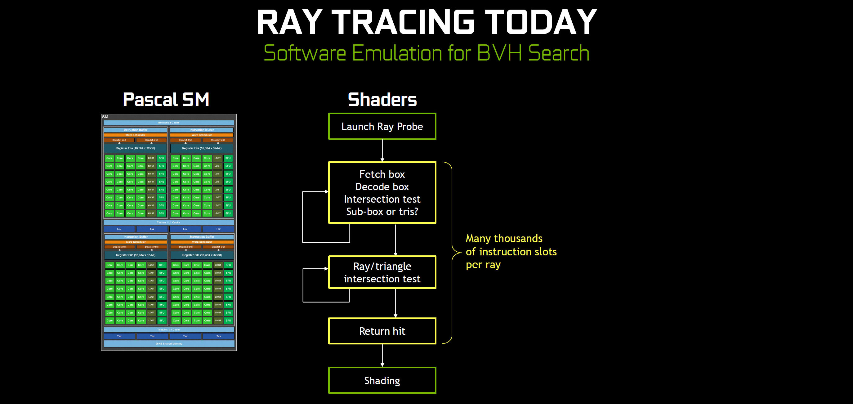
It's important to state that these RT TFLOPS are not general purpose TFLOPS, but instead these are specific operations designed to accelerate ray-tracing calculations. The RT cores compute ray triangle intersections (where a ray hits a polygon), as well as BVH traversal. That second bit requires a lengthier explanation.
BVH stands for "bounding volume hierarchy" and is a method for optimizing intersection calculations. Instead of checking rays against polygons, objects are encapsulated by larger, simple volumes. If a ray doesn't intersect the large volume, no additional effort needs to be spent checking the object. Conversely, if a ray does intersect the bounding volume, then the next level of the hierarchy gets checked, with each level becoming more detailed.
All of the BVH calculations can be done using shader cores, but Nvidia says it takes thousands of shader calculations per ray, during which time the CUDA cores can't be working on other stuff. The RT cores offload all of that and run independently with the CUDA cores, so on the Turing architecture enabling ray tracing won't completely tank performance.

The final major architectural feature in Turing is the inclusion of Tensor cores. Normally used for machine learning, you might wonder why these are even useful for gaming. I'll have a separate piece digging deeper into the machine learning aspects of Turing, but in short there's a lot of future potential.
Nvidia has worked with Microsoft to create the DirectML and Windows ML (DirectX Machine Learning) APIs, so this is something with broad industry support. Future games could use machine learning to enhance AI in games, offer improved voice interfaces, and enhance image quality. Those are all longer term goals, however—especially when for the next five or more years a large installed base of gamers won't have Tensor cores available. In the more immediate future, these cores can be used in more practical ways.
Nvidia showed some examples of improved image upscaling quality, where machine learning that has been trained on millions of images can generate a better result with less blockiness and other artifacts. Imagine rendering a game at 1080p with a high framerate, but then using the Tensor cores to upscale that to a pseudo-4k without the massive hit to performance we currently incur. It wouldn't necessarily be perfect, but suddenly the thought of 4k displays running at 144Hz with 'native' 4k content isn't so far-fetched.
The Tensor cores are also required to handle an AI-trained denoising algorithm for ray tracing. While the Tensor cores are running, the rest of the GPU basically ends up being idle, so unlike the RT cores and INT/FP pipelines the Tensor cores don't really work concurrently. However, Nvidia suggests that DLSS and denoising could run with only 20 percent of the total frame time.
At a hardware level, the Turing architecture Tensor cores also add a few new tricks compared to those in Volta. Specifically, native support for INT8 and INT4 workloads allows for potentially double or quadruple the computational performance relative to FP16/FP32 hybrid models. These may not be immediately applicable to graphics workloads, which are more susceptible to quantization, but research into alternative machine learning algorithms is ongoing.

RTX-OPS, a new performance metric
With all of the changes in the Turing architecture, comparing performance between various GPU generations just became a lot more difficult. For existing games and workloads that don't leverage the new features, the old FP32 TFLOPS figure might still be somewhat okay, but the superscalar design (ie, the ability to dispatch multiple concurrent instructions) muddies even those figures. To help compare things, Nvidia devised a new performance metric, RTX-OPS.
Obviously this will favor the RTX GPUs, but the general idea isn't that bad. In a modern game that fully implements ray tracing effects with DLSS and denoising, the above slide shows how the average workload gets distributed. 80 percent of the time is spent on FP32 shading (what games currently do), with 35 percent of that time also having concurrent INT32 shading work. Ray tracing calculations meanwhile use another 40 percent of the time, and the final output gets post-processed by the Tensor cores taking a final 20 percent.
With that formula in hand, the GeForce RTX 2080 Ti FE ends up with 78 RTX-OPS, as shown. How would a GTX 1080 Ti compare? It lacks the Tensor cores and RT cores and can't do simultaneous INT32 + FP32 calculations, so everything uses the base TFLOPS figure and just uses a different slice of the overall pie. In other words, GTX 1080 Ti has RTX-OPS equal to its TFLOPS figure of 11.3.
Does that mean the RTX 2080 Ti is nearly seven times faster than the 1080 Ti? Not really, but in future workloads that use ray tracing and machine learning code, previous architectures simply won't be able to compete.


Turing architecture: GDDR6 and improved L1/L2 cache
Improving overall GPU performance is great, but faster GPUs also need more memory bandwidth. To keep the GPUs fed with data, Nvidia has moved to GDDR6 memory and reworked the cache and memory subsystem in the Turing architecture. L1 cache bandwidth is doubled, and the L1 cache can now run as either 32K L1 and 64K shared memory, or 64K L1 and 32K shared memory. That potentially increases the L1 cache size 167 percent relative to Pascal. L2 cache size has also been doubled, and Nvidia states that the L2 cache delivers "significantly higher bandwidth" as well.
The improved clockspeeds of GDDR6 relative to GDDR5 and GDDR5X would help, but Turing doesn't stop there. We know Pascal already had several lossless memory compression techniques available, and the Turing architecture continues to improve in this area. Nvidia doesn't provide specific details on what has changed, but the larger caches and improved compression increase the effective bandwidth by 20-35 percent relative to Pascal GPUs.
Combined, the GeForce RTX 2080 Ti on average has 50 percent more effective bandwidth than the GTX 1080 Ti, even though memory speeds are only 27 percent faster. The RTX 2080 and 2070 should show even greater improvements, since the memory clocks have increased by 40 and 75 percent, respectively.


Turing architecture: even more enhancements
There's so much new stuff in Turing that it's hard to say how much any one aspect will matter in the long run. The Pascal and Maxwell architectures likewise had some new features—anyone remember VXAO, Voxel Ambient Occlusion, which to my knowledge was only used in two games (Rise of the Tomb Raider and Final Fantasy XV)? There's potential for these other features to be useful as well, but I'm grouping all of them together in the above gallery and this short description.
Mesh shaders are the next iteration of vertex, geometry, and tessellation shaders. The main idea here is to move LOD (Level of Detail) calculations from the CPU and onto the GPU. This can improve performance by orders of magnitude, and Nvidia showed a demonstration of a ship flying through a massive asteroid field with mesh shaders allowing for the real-time use of 'trillions' of polygons. The catch is that the LOD scaling culls that down to a more manageable number, in the millions instead of trillions. Mesh shaders will be an extension to existing graphics APIs for now, so they're less likely to see widespread use until/unless they're directly integrated into the DIrectX/Vulkan APIs, but the demo looked very cool.
Variable Rate Shading (VRS) is the next new feature, and it allows games to use more shaders where needed, and fewer shaders where it's not important. The goal is to provide equivalent image quality with better performance, and Nvidia suggested a 15 percent boost in performance should be possible. VRS can also be used in multiple ways, like MAS (Motion Adaptive Shading) where fast moving objects don't require as much detail (because they end up being blurred), and CAS (Content Adaptive Shading) where more effort is spent on complex surfaces like a car in a driving game, and less effort is used on simple surfaces like the road in the same game.
Nvidia showed a modified build of Wolfenstein II running with CAS and the ability to toggle the feature on/off. Without spending more time pixel peeping, I can say that there was no immediately visible difference between the two modes, but CAS did improve performance slightly. Whether we'll see a public patch to the game or not remains to be seen, and again this is something less likely to see widespread use.
Finally, Nvidia briefly discussed two more features in the Turing architecture: Multi-View Rendering (MVR), an enhanced version of the Simultaneous Multi-Projection (SMP) that was already a feature in Pascal, and Texture Space Shading (TSS). Where SMP primarily focused on two views and VR applications, MVP can do four views per pass and removes some view dependent attributes. It should help to further improve performance in VR applications, especially with some of the newer VR headsets that have a wider field of view.
TSS meanwhile makes even less sense to those of us not actively writing game engines. Nvidia says it can allow developers to exploit both spatial and temporal rendering redundancy, effectively reducing the amount of shader work that needs to run. There are several pages in the Turing architecture whitepaper describing use cases for TSS, but as with previous technologies like SMP and VXAO, it remains to be seen how many developers will use the feature.

Turing architecture: improved NVENC for videos
Outside of the GPU and memory enhancements, Nvidia has also worked to improve NVENC, the hardware used for video encoding/decoding. Pascal GPUs delivered good performance but the quality of the resulting videos wasn't always as good as even the x264 Fast profile running on a CPU. With Turing, Nvidia claims to deliver equal or better quality than x264 Fast, with almost no CPU load.
If you're streaming at 1080p, this won't matter much since Pascal could handle that resolution fine, and a good CPU could run x264 Fast encoding with only a modest overhead. Moving up to 4k and higher bitrates is a different matter, with CPU utilization spiking and a large number of dropped frames. Turing aims to deliver 4k encoding with almost no CPU impact.
Outside of streaming use, the Turing architecture also adds support for 8k30 HEVC HDR encoding, and can also deliver equivalent quality to Pascal at 15-25 percent lower bitrates for HEVC and H.264 content. For decoding, Turing adds support for VP9 10/12b HDR content and HEVC 444 10/12b HDR.

Turing architecture: manufactured using TSMC 12nm FinFET
The Turing architecture advancement are largely thanks to improvements in manufacturing technologies. Turing GPUs will be manufactured using TSMC's 12nm FinFET process. While TSMC 12nm FinFET is more of a refinement and tweak to the existing 16nm rather than a large reduction in feature sizes, optimizations to the process technology over the past two years should help improve clockspeeds, chip density, and power use—the holy trinity of faster, smaller, and cooler running chips. TSMC's 12nm FinFET process is also mature at this point, with good yields, which allows Nvidia to create such large GPUs.
Even with the process improvements, TU102, TU104, and TU106 are all very big. The TU104 as an example is only slightly smaller than the GP102 used in the GTX 1080 Ti. Further driving home the fact that 12nm is more marketing than an actual shrink, GP102 has 12 billion transistors compared to TU106's 10.8 billion transistors. That's 11 percent more transistors in the GP102, with a die size that's eight percent larger.
There's hope for future improvements sooner rather than later as well. TSMC is already close to full production for its 7nm process, and AMD's Vega 7nm Radeon Instinct GPUs are supposed to ship by the end of 2018. If TSMC 7nm works well, we could see a die shrink of Turing by late 2019. Maybe it will be called Ampere, maybe it will be something else. Not only would 7nm bring sizes down to more manageable levels, but Nvidia could double down on RT cores or other features.

Nvidia's Turing architecture is a game changer
With everything new in the Turing architecture, it's easy to see why Nvidia is calling this the biggest leap in graphics architectures the company has ever created. Real-time ray tracing or something similar has always been the pie in the sky dream of gamers. That dream just jumped 5-10 years closer.
Our graphics chips have come a long way in the past 30 years, including milestones like the 3dfx Voodoo as the first mainstream consumer card that could do high performance 3D graphics, the GeForce 256 as the first GPU with acceleration of the transform and lighting process, and AMD's Radeon 9700 Pro as the first fully programmable DirectX 9 GPU. Nvidia's Turing architecture looks to be as big of a change relative to its predecessors as any of those products.
Like all change, this isn't necessarily going to be a nice and clean break with the old and the beginning of something new. As cool as real-time ray-tracing might be, it requires new hardware. It's the proverbial chicken and egg problem, where the software won't support a new feature without the hardware, but building hardware to accelerate something that isn't currently used is a big investment. Nvidia has made that investment with RTX and its Turing architecture, and only time will tell if it pays off.
For at least the next five years, we're going to be in a messy situation where most gamers don't have a card that can do RTX or DXR ray tracing at acceptable performance levels—with or without machine learning Tensor cores to help with denoising. The good news is that DXR leverages many of the data structures already used in Direct3D, so adding some ray tracing effects to a game shouldn't be too difficult. That's good news, because most game developers will need to continue supporting legacy products and rasterization technologies. Hybrid rendering will be with us for a long time, I suspect.
As cool as ray tracing is, I also have to wonder if the machine learning capabilities in Turing may prove to be even more important. Deep learning is revolutionizing diverse fields including science, medicine, automotive, and more. I'm not convinced DLSS will really look as good as native 4k rendering, but then I can also say that the difference between 4k and 1440p in many games isn't nearly as great as you might expect. I'm cautiously optimistic, though, and even more so for things like improved AI, anti-cheat, and other potential uses.
The Turing architecture is a tour de force from the leading graphics technology company. It's far more than I expected to see when Volta was launched last year for supercomputers. It's also shocking how quickly the GV100 just lost most of its appeal. GeForce RTX 2080 Ti for $1,199 is a lot to ask, but it's also a helluva lot better deal than a Titan Xp for that same price, or a Titan V for $2,999.

But all the theoretical improvements for now don't make the GeForce RTX cards substantially faster than the existing Pascal solutions. In fact, the GTX 1080 Ti and RTX 2080 are effectively tied in most games, except the RTX card costs $100 more. The current situation brings to mind the transition from DirectX 7 (hardware transform and lighting) to DX8/DX9 (fully programmable shaders), where we had to wait years before the games properly utilized the new features. There are already more ray tracing games slated to launch in the next six months than early DX8 titles, but we're still left waiting for at least a month or two before we get to see the RT cores properly utilized in a game.


