Join The Club


After months of rumours, leaks, and tidbits from the company itself, Intel finally announced its Panther Lake CPUs at its regular Technology Tour event, this time in Arizona, US. It was an appropriate location to do so, as the US state is also home to multiple Intel foundries, and Fab 52 is one of two that operate its newest process node: Intel 18A.
This particular semiconductor chip production method is responsible for making the key tile, or chiplet, that lies at the heart of every Panther Lake processor. But where Intel's previous tiled architectures, Meteor Lake (MTL) and Arrow Lake (ARL), sported one design apiece, Panther Lake or PTL for short, comes in three varieties.
The Panther Lake trio

With Meteor Lake, Lunar Lake, and Arrow Lake, Intel created a single processor design and used binning strategies to create broad processor families from them. For example, one LNL chip can be found in nine different Core Ultra 200V CPUs.
Article continues belowNot so with Panther Lake, because while binning will still be used to produce all the different models (i.e. some will have disabled cores, others will just be clocked lower), there are three chip designs in total.
- PTL '8 core': 4 P-cores, 4 LPE-cores, 4 Xe3 cores, 12 PCIe lanes
- PTL '16 core': 4 P-cores, 4 LPE-cores, 8 E-cores, 4 Xe3 cores, 20 PCIe lanes
- PTL '16 core 12Xe': 4 P-cores, 4 LPE-cores, 8 E-cores, 12 Xe3 cores, 12 PCIe lanes
This isn't just one chip with disabled bits to make the others; Intel is using multiple tiles to create these configurations. Making things more complicated to explain is the fact that Intel has also created two different tiles for each of the primary sections: compute, graphics, and platform controller. To better understand how each PTL variant differs, let's consider the new tiles separately.
Panther Lake compute tile

Starting with arguably the most important chiplet in Panther Lake, Intel's new compute tile is going to be under close scrutiny in the coming months. That's because no small part of what makes the compute tile special is down to the 18A process node, with its gate-all-around RibbonFET nanoscale switches and PowerVia backside power delivery.
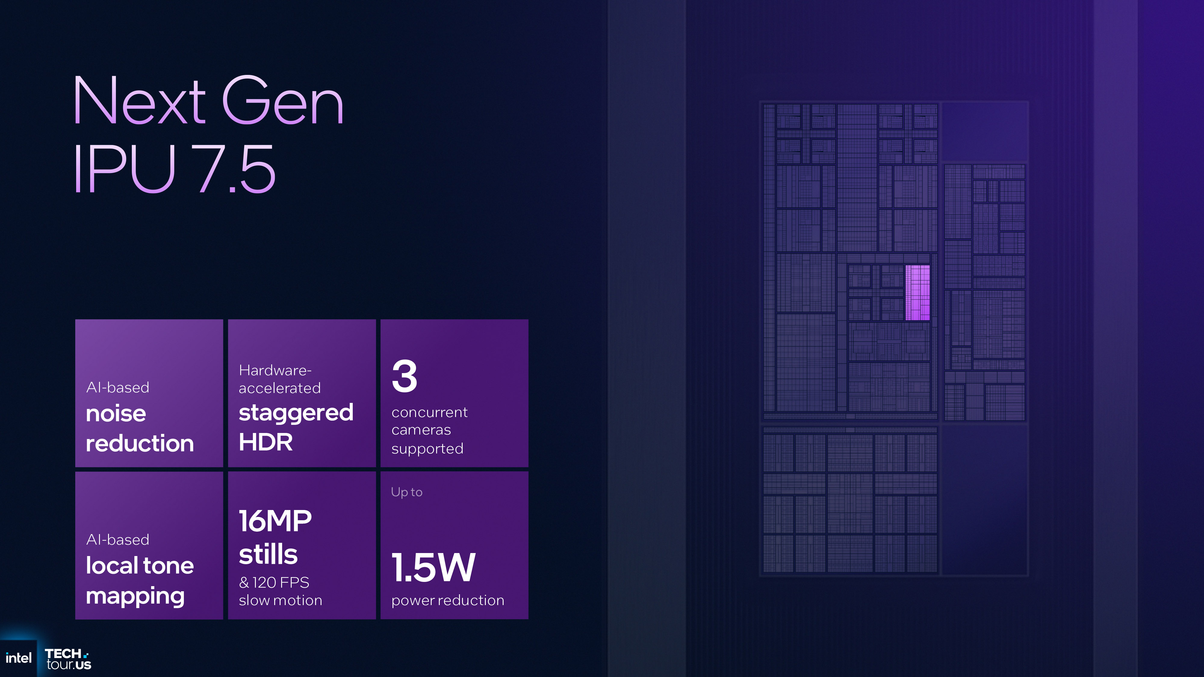
Both compute tile versions house P-cores and E-cores, along with Intel's latest NPU (neural processing unit), an updated IPU (image processing unit), media and display engines, plus the DRAM controllers and interfaces. The last aspect is a notable improvement over Arrow Lake, which has the memory system in a separate tile from the compute one, which isn't good for achieving low latencies.
There's also 8 MB of 'memory-side' cache that's accessible by all cores. It's a bit like an L4 cache, but it's better to think of it as being an ultra-fast buffer for handling data transfers between RAM and the various clusters of cores, rather than an all-encompassing cache. It's designed to help reduce traffic on the memory bus, as well as improve overall latencies within the processor.
Intel doesn't have a codename for the different compute tiles, so I'll just refer to them as 'small' compute and 'large' compute, although there's not a huge size discrepancy between them.
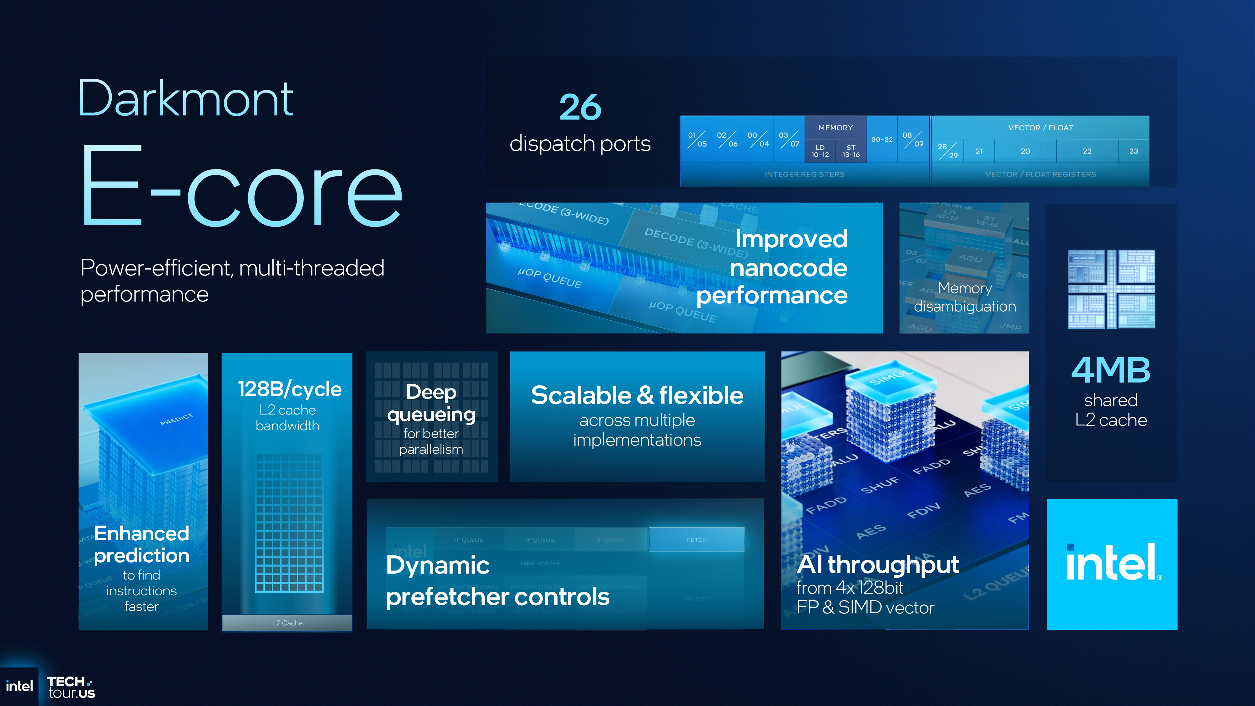
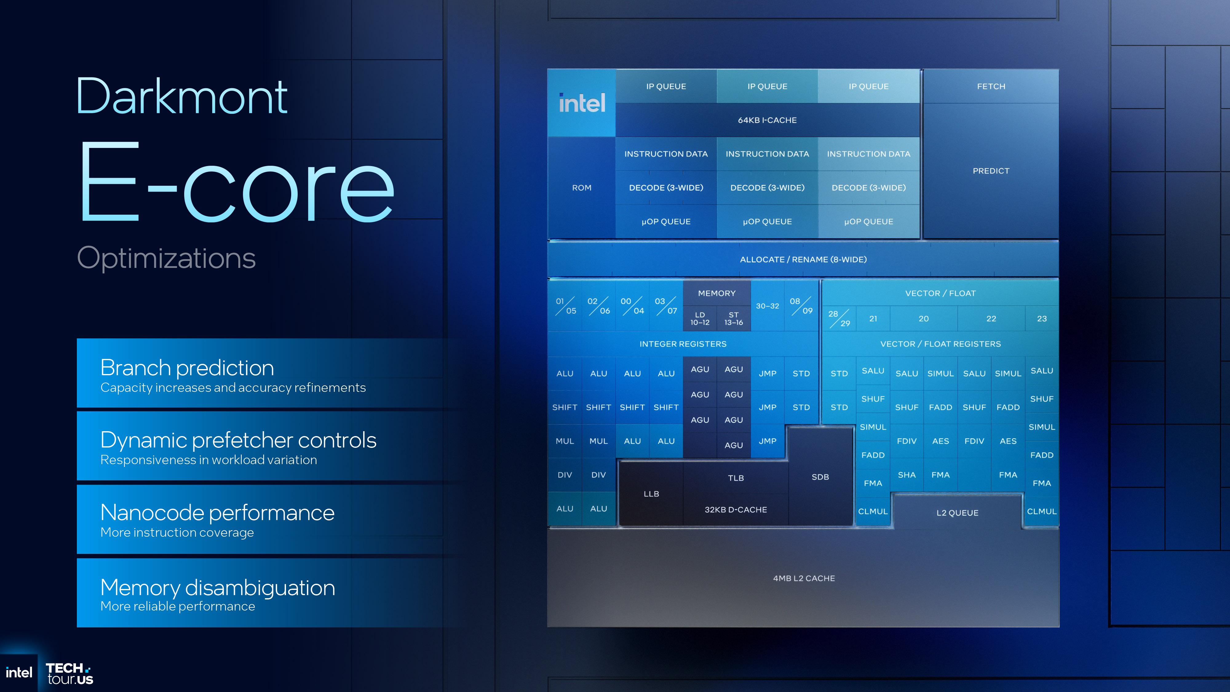
Both of them house four Darkmont Low Power E-cores in a separate 'island' within the tile, but where small compute only sports a further four Cougar Cove P-cores, big compute boasts an additional eight Darkmont E-cores, grouped right next to the P-cores.
It's fair to say that the new P- and E-cores aren't a revolution in CPU architecture; instead, they're a small, evolutionary step up from previous designs, sporting a variety of improvements to achieve more performance, at the same clock speeds and power, as before.
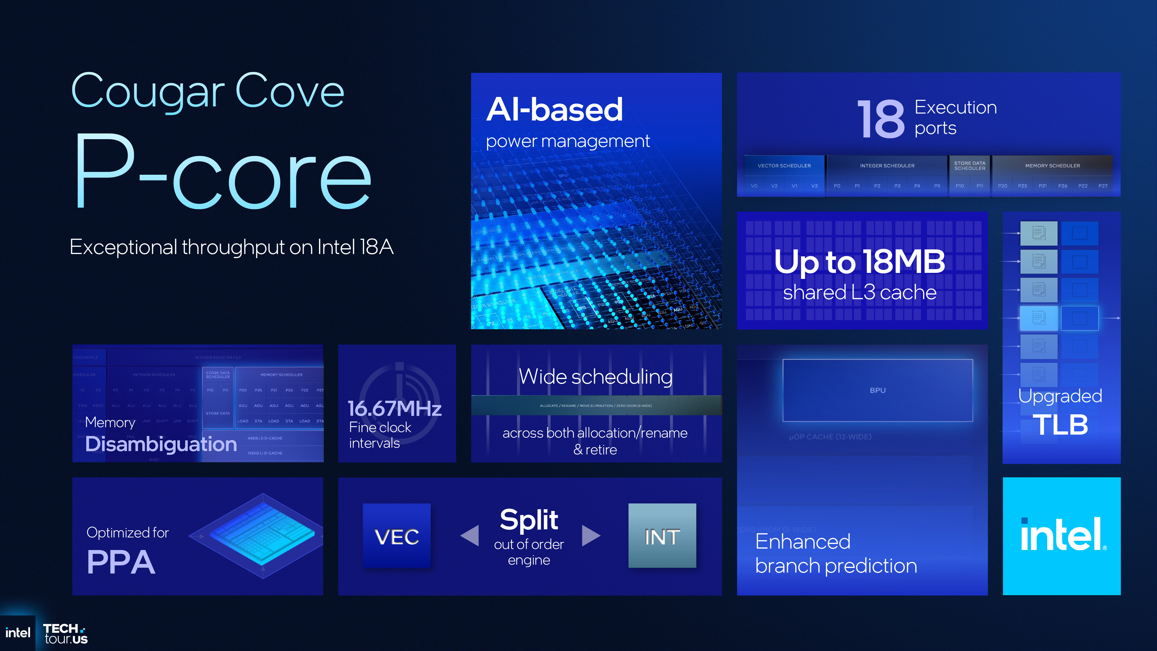
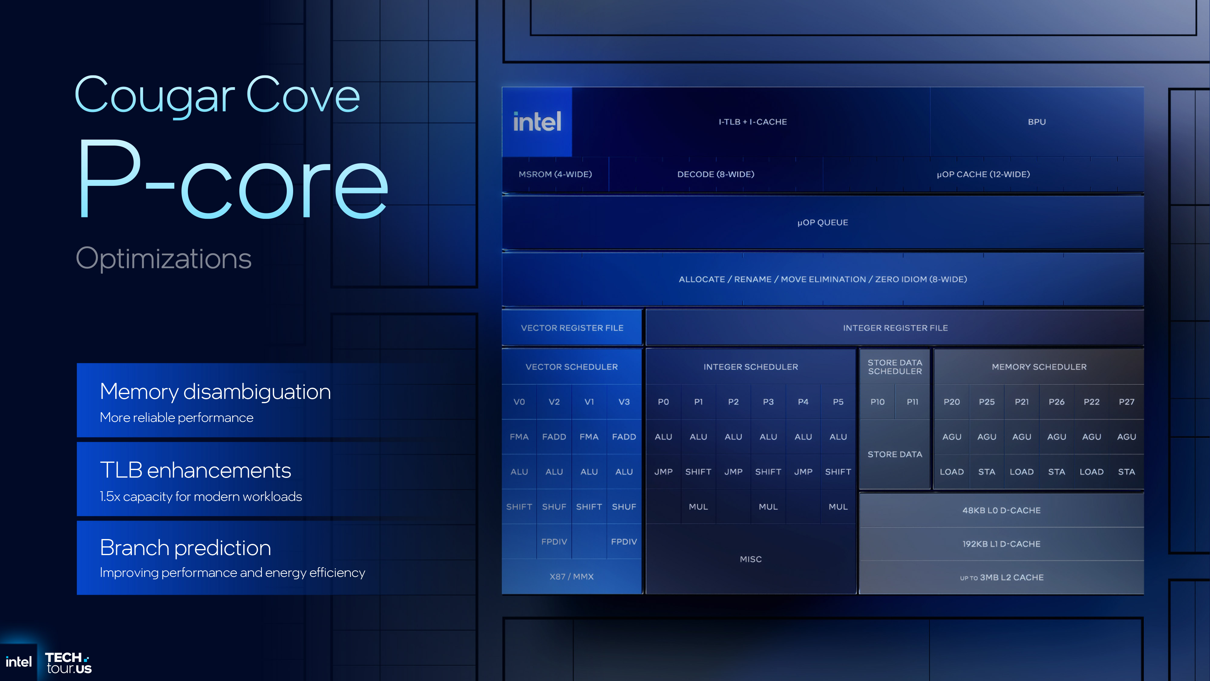
For example, Cougar Cove gets a 50% larger TLB and a better branch prediction unit. The former is a translation lookaside buffer, which speeds up memory requests by storing the most recent address translations (virtual to physical), whereas the latter reduces thread stalls by calculating what instructions and data are most likely to be processed next.
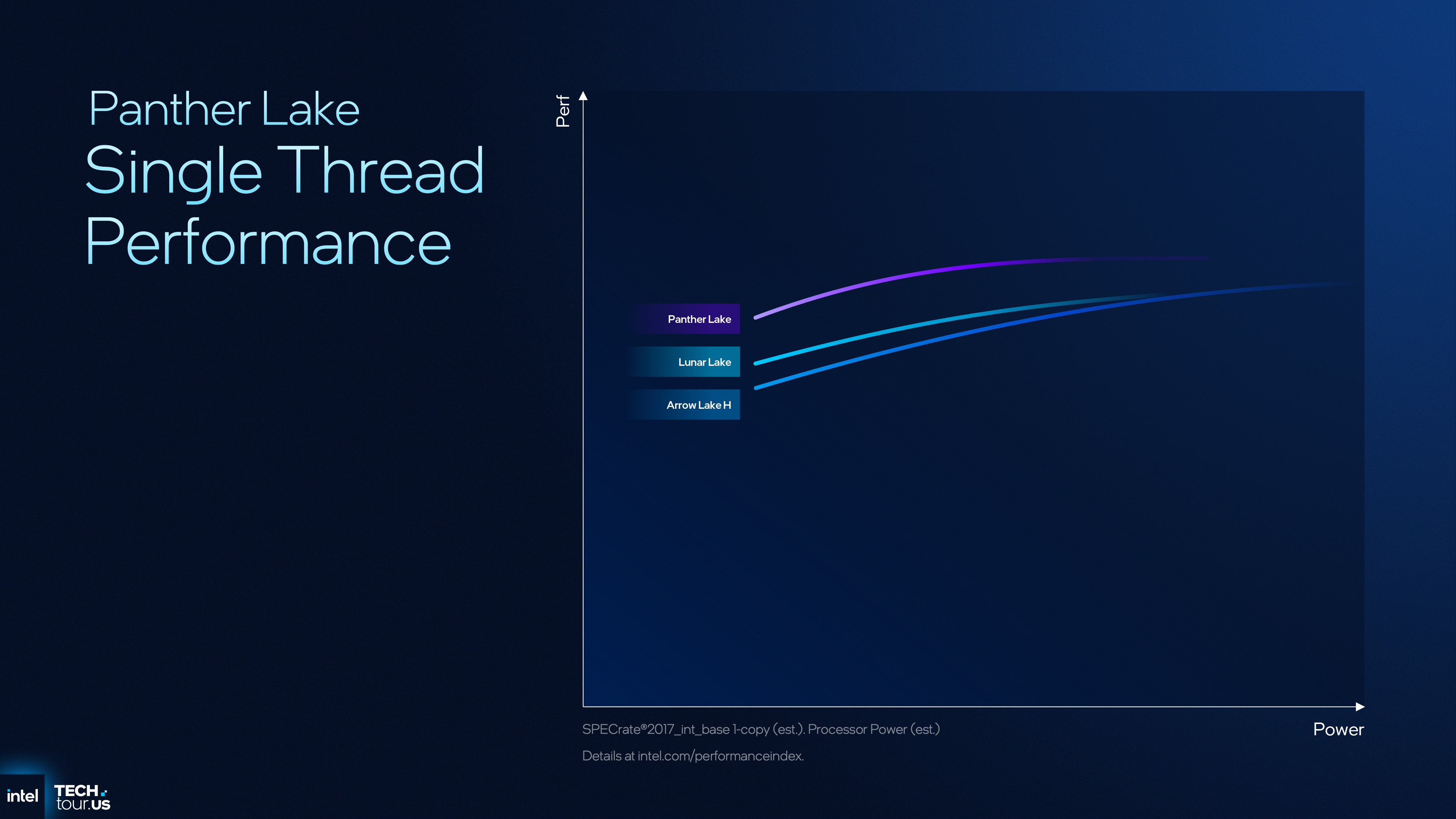
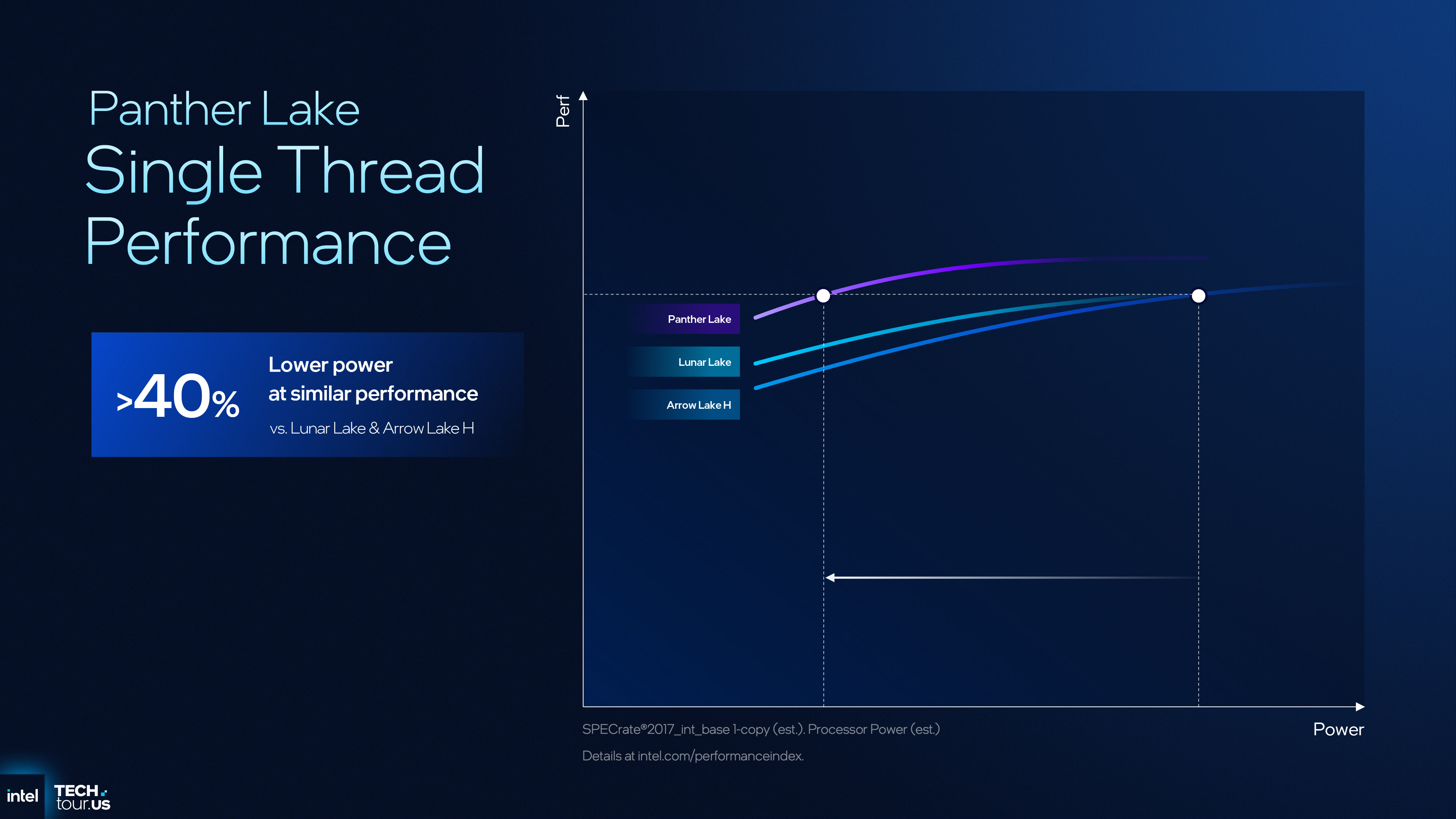
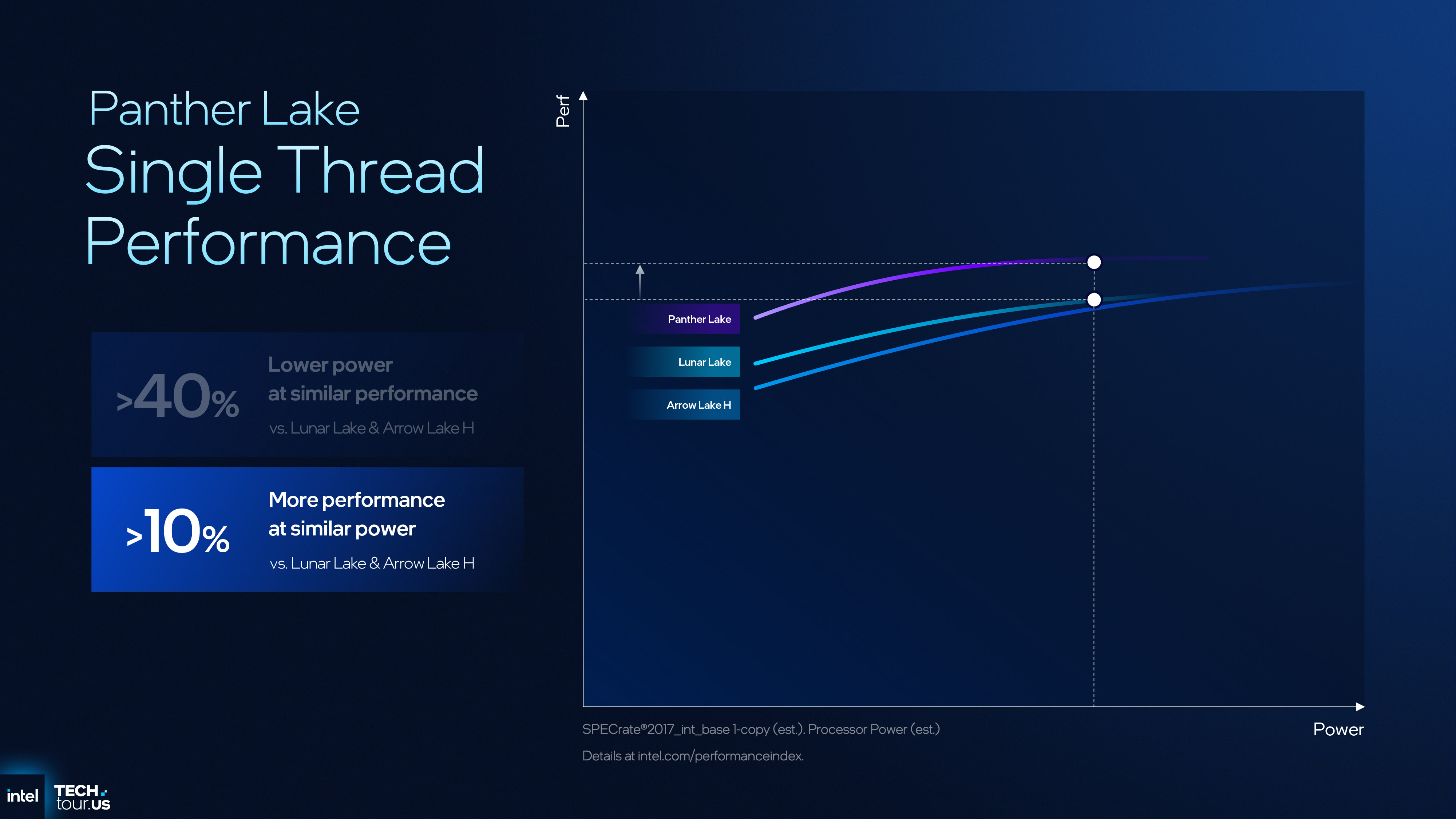
It's a similar story with Darkmont: better branch prediction and prefetch, more instructions covered by the nanocode cache, and a wider data bus to the L2 cache. By themselves, none of the changes are major, but taken altogether, Cougar Cove and Darkmont give Panther Lake roughly 10% better single-threaded performance, compared to LNL and ARL-H.
The NPU is a lot more compact, thanks to the 18A process node and a fresh design, though your average PC user is perhaps still waiting for that 'killer app' to make an AI-capable CPU a must-buy. However, in the edge market (Intel describes this as everything that isn't PC or server), the 50 TOPs peak output of the NPU, in such a small, low-power package, will be greatly appreciated.
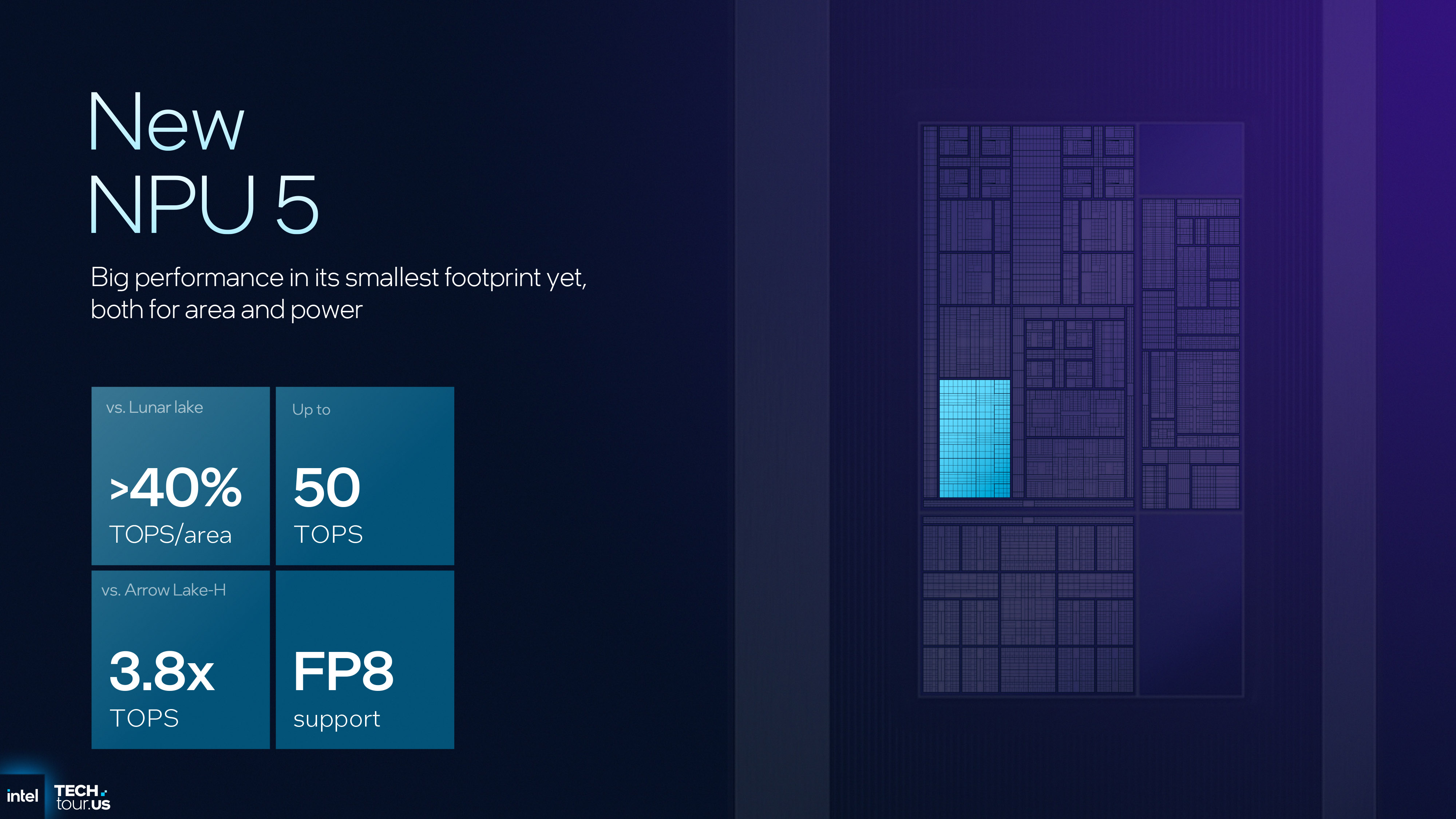
Combined with the cores and the GPU, Panther Lake as a whole can achieve up to 180 TOPs (trillions of operations per second). That's 50% more than Lunar Lake and a massive 400% better than Arrow Lake, though the latter only has a tiny NPU and iGPU. Like every other chip company, Intel is betting heavily on AI, so improvements in this area were to be expected.
This is also why the compute tile houses the DRAM controllers and interfaces, and the most capable PTL variant supports up to 96 GB of LPDDR5x-9600 or 128 MB of DDR5-7200. That's a little better than AMD's best APUs, the Ryzen AI 9 HX 375 and Max+ 395, which support up to LPDDR5x-8000, but the best news is that, unlike Lunar Lake, the DRAM is no longer on package, so more vendors will be willing to use it.
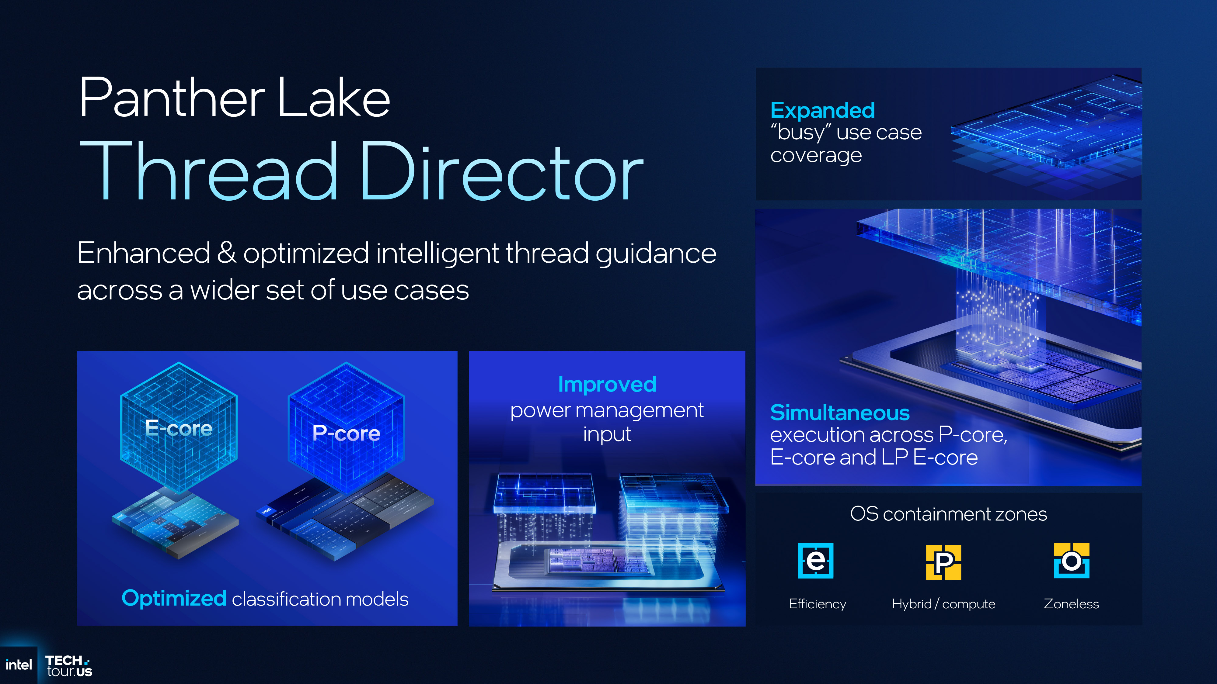
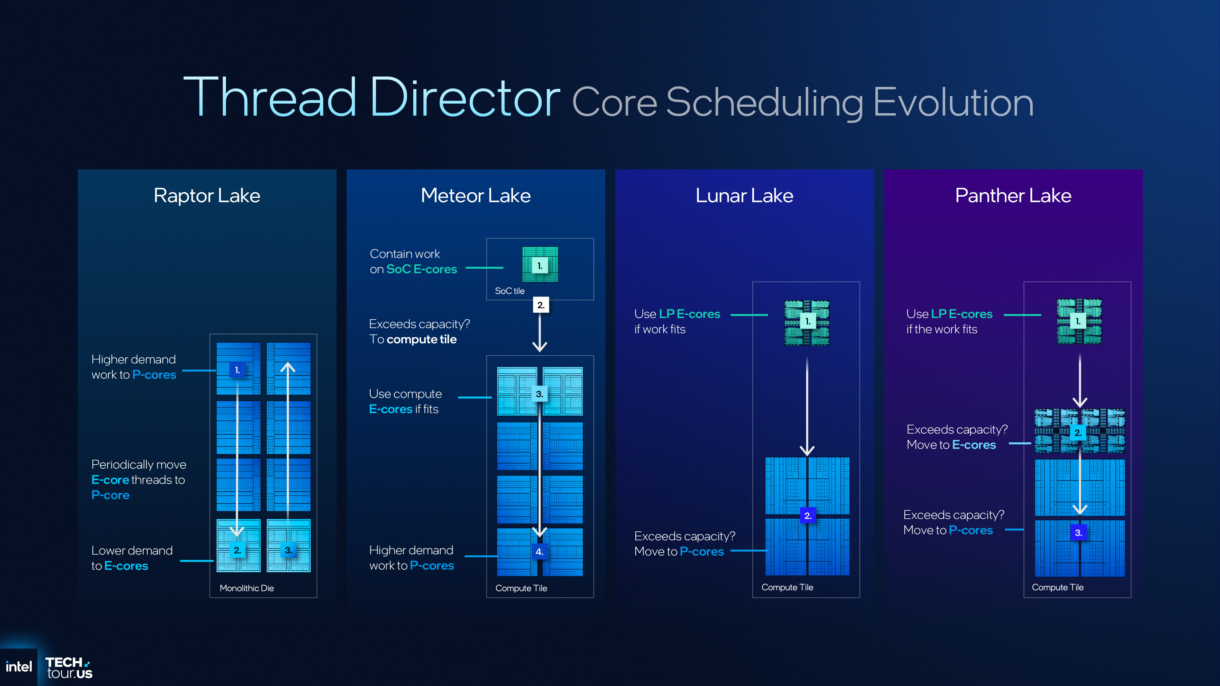
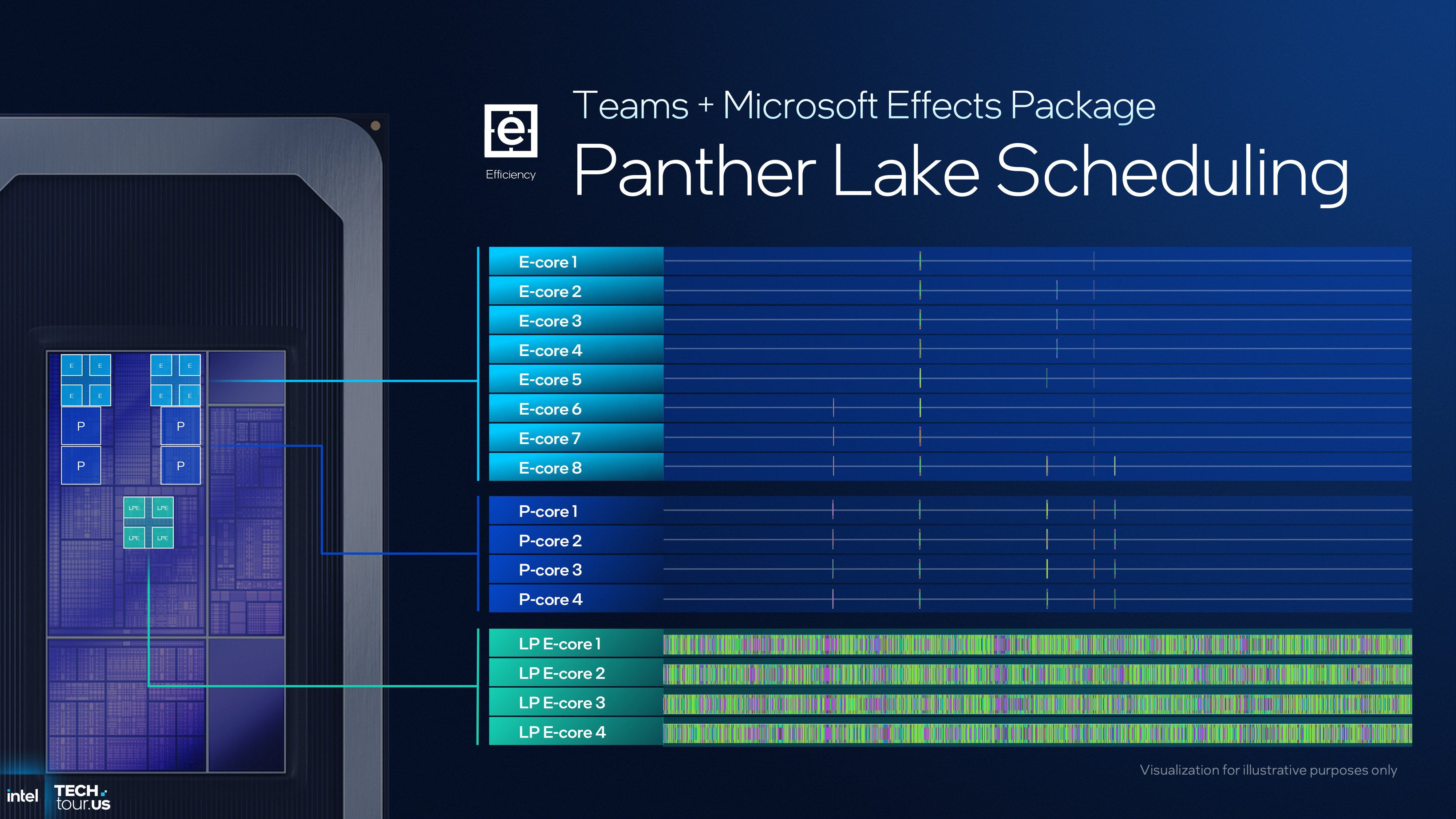
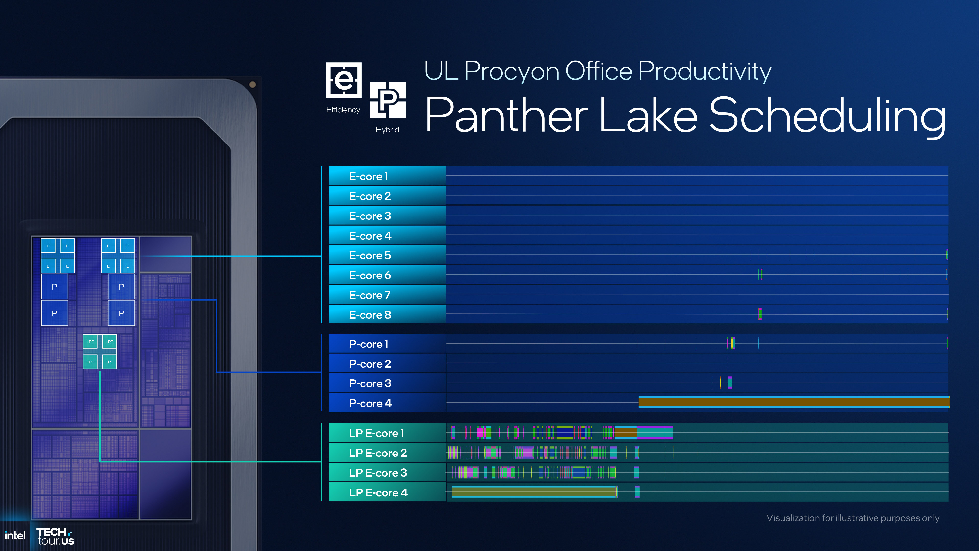
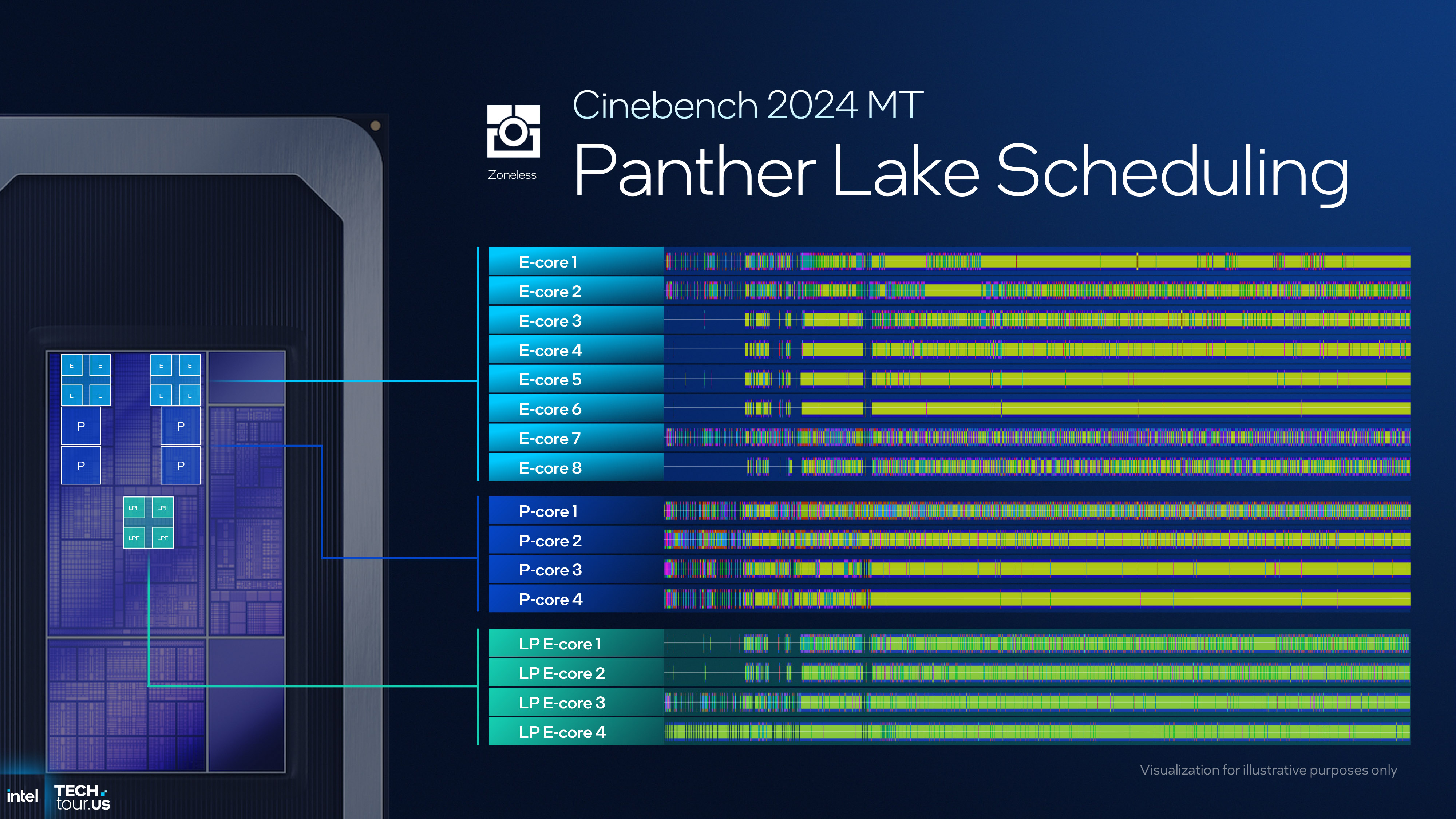
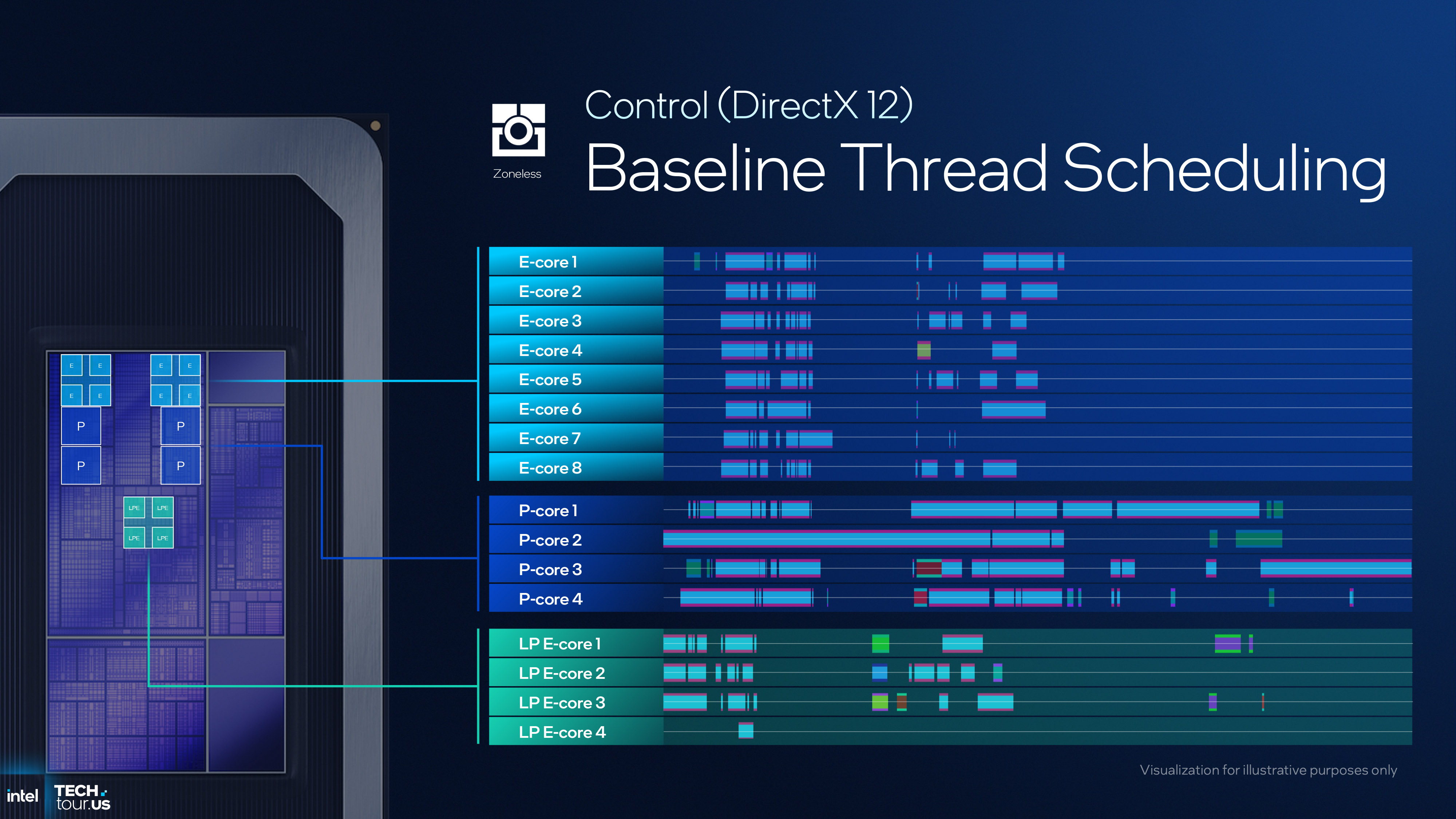
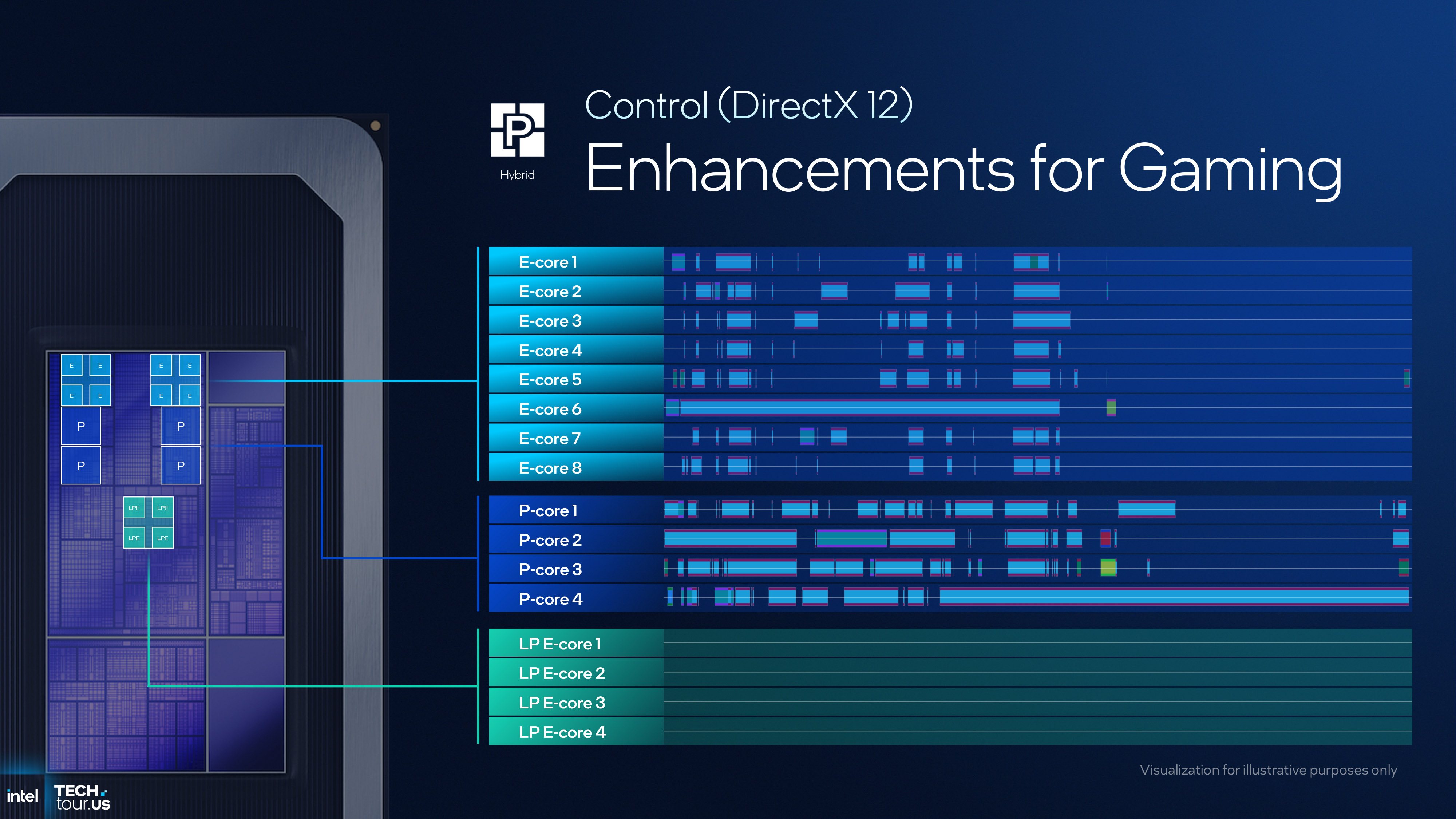
Adding better cores, more cache, and faster RAM is all well and good, but PTL's fundamental layout demands top-notch thread scheduling to maximise performance. Where AMD's processor cores are all the same in each architectural generation, Intel's P- and E-cores are very different.
Fortunately, the Thread Director part of the new compute tile has been given a thorough overhaul and Intel is claiming some pretty significant gains in how well threads are scheduling on its hybrid chip.
This is especially true for gaming, where better power management also kicks in, ensuring that a game's threads are correctly sent to the right core and the iGPU gets the lion's share (or should that be panther's share?) of the available power.
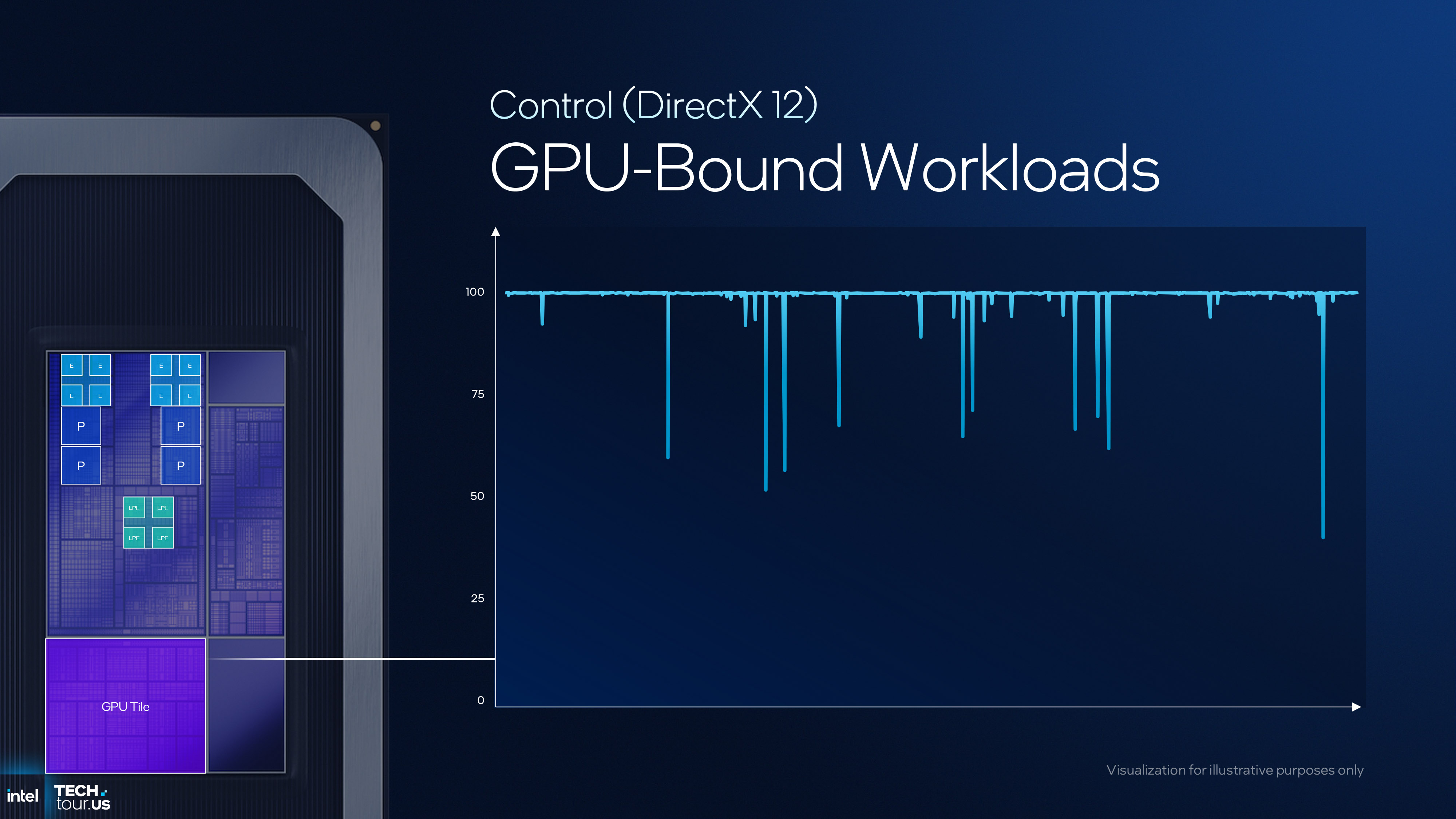
Xe3 graphics (GPU) tile

Following on from Meteor Lake and Arrow Lake, Panther Lake's integrated graphics processor is a separate tile all by itself, though the media and display engines are within the compute tile to improve latencies and power efficiency when running videos.
I've covered all the important details about the new GPU architecture, Xe3, in a separate article, but to summarise briefly here, it's a bit like the CPU cores: small improvements rather than a wholesale change in direction.
Just as with compute tile, Intel has created two GPU tiles. The smallest is fabricated on its own Intel 3 process node, and it really is small, just 4 Xe3 cores (512 shaders) hooked up to 4 MB of L2 cache. That's the same size as Arrow Lake's iGPU (which is half as small as Lunar Lake's), but the base PTL configuration isn't really designed to be a gaming powerhouse.

That honour goes to the other GPU tile, as it boasts 12 Xe3 cores (1536 shaders) and a whopping 16 MB of L2 cache. Per core, that's 48% more cache than in any Battlemage graphics card.
Along with the architectural improvements, better memory latencies, and faster RAM support, and the fact that it's made on TSMC's N3E process node, the 12Xe PTL chip is going to be a serious contender for the best processor for handheld gaming PCs.
Platform controller tile
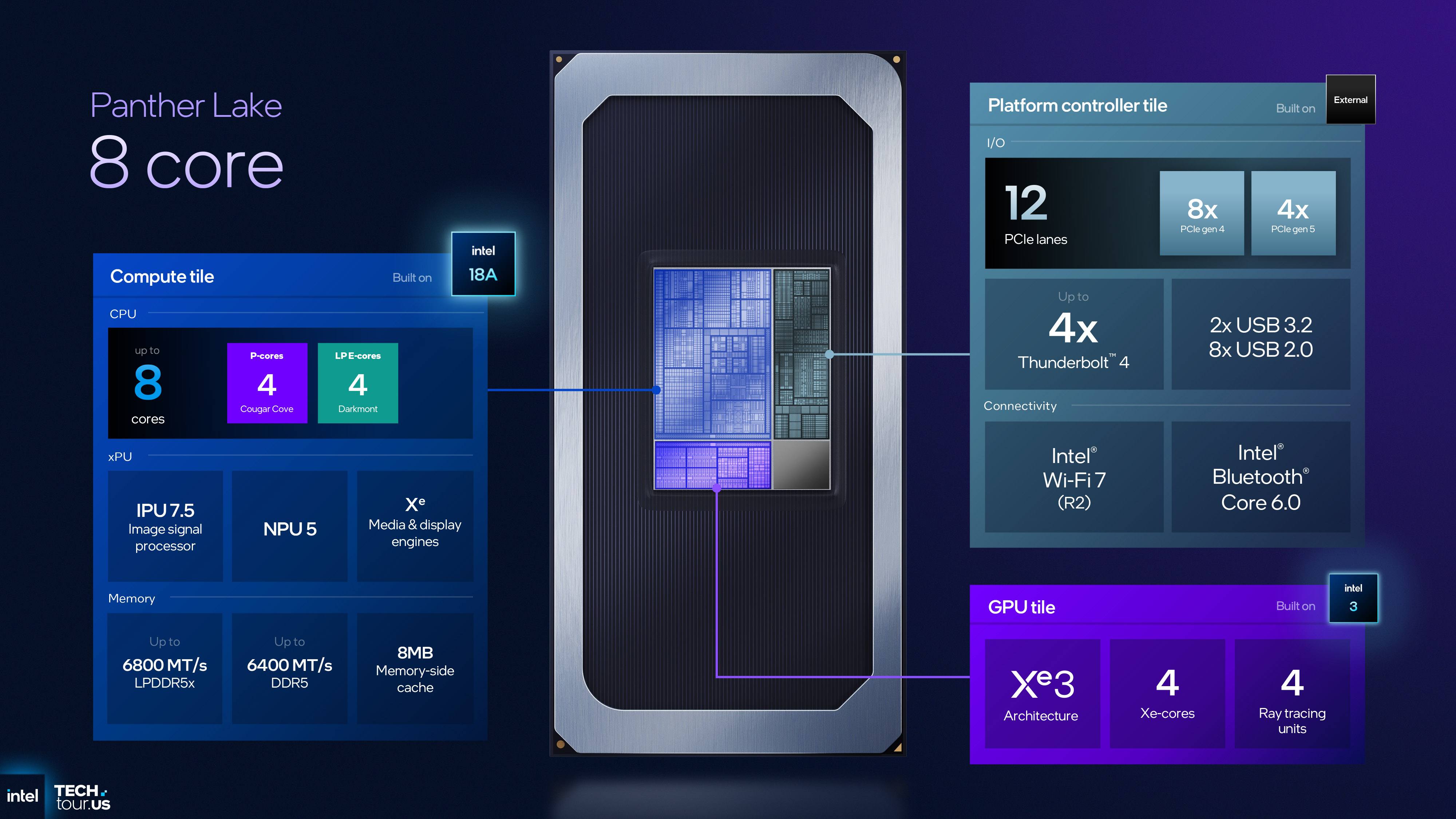
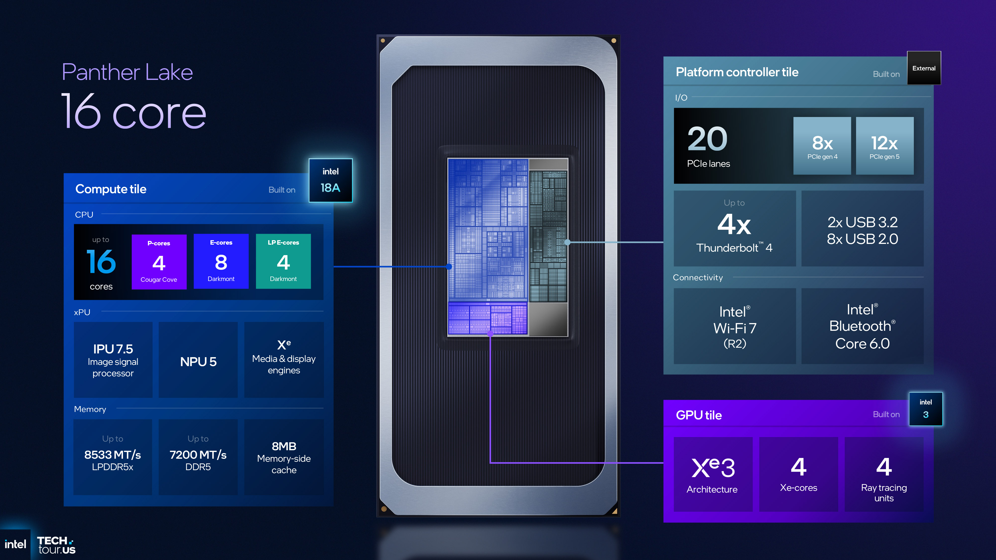
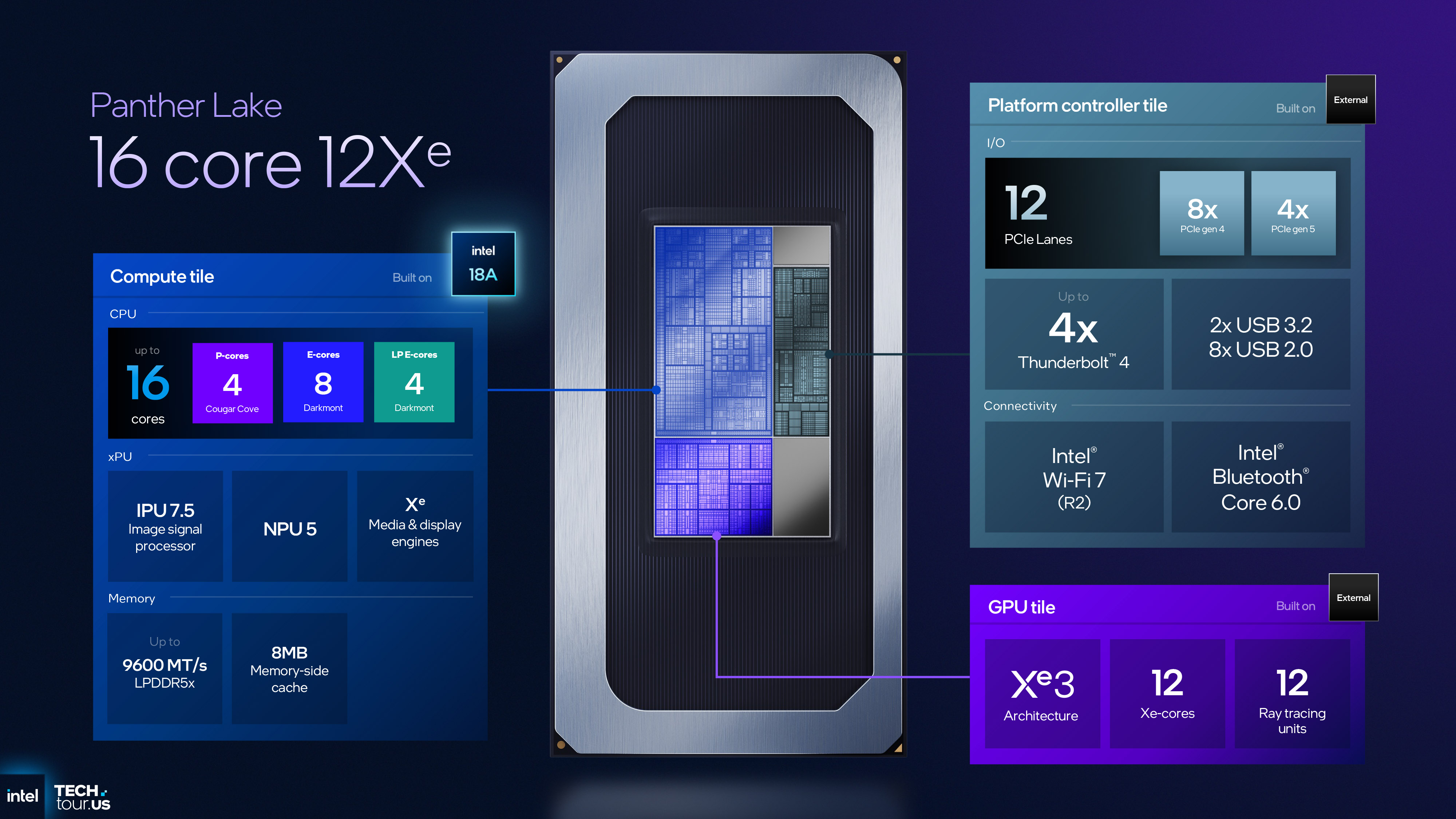
Unlike the compute and graphics tiles, the two platform controller designs are very similar and differ only in terms of the number of PCIe lanes. Packed inside both of them are Thunderbolt 4, USB 3.2, and USB 2.0 controllers for up to four, two, and eight ports, respectively. It might seem disappointing to see that USB4 doesn't feature, but TB4 is fully compatible with USB4 anyway, and is just as fast (if one ignores USB4's 80 Gbps mode, which is barely supported at the moment).
When it comes to PTL's PCI Express features, the smaller platform controller only offers 12 lanes, four of which are PCIe 5.0 and the remaining eight being Gen 4. The bigger tile has 20 lanes in total, adding a further eight Gen 5. The base PTL layout and the 12Xe version use the small tie, with the 16-core 4Xe one using the larger. Why? Because it's expected to hand over eight PCIe lanes to connect to a discrete GPU.
The platform controller tile also houses a second-generation Intel Wi-Fi 7 module, along with Bluetooth Core 6.0 and Bluetooth LE. These are just the MACs (medium access controls) and the physical interfaces for both wireless connections are housed in the motherboard chipset.

Intel claims its new Wi-Fi 7 module is significantly better than its first iteration, though with so many variables affecting wireless performance, you may find your new Panther Lake laptop no better in this aspect.
You should, however, find Bluetooth to be a lot better. Intel claims its new system now has twice the range of the previous BT modules, along with better features for audio streaming over BLE.
It might come as a surprise to learn that the platform controller tiles are manufactured on TSMC's N6 process node, something that's five years old and essentially nothing more than a tweaked N7. However, the tile contains a lot of analogue circuitry for all the PCIe and USB signals, and that scales very poorly with node shrinks.
Had Intel used something like N3 to make the platform controller tile, it would only be a fraction smaller, run no better, and cost an awful lot more to make. In other words, N6 is the sensible choice.
Putting the tiles all together

In many ways, Panther Lake as a whole is a sensible choice. Sure, we'd all like more P-cores in the compute tile, but rather than that, Intel has instead focused on improving its thread scheduler and power management system to ensure that threads go to the right cores.
A USB4 controller would be neat, too, but that would make the platform controller tile bigger and more costly, and not every laptop needs that kind of port at the moment. For those that do, it can be implemented via the motherboard.
Intel could have copied AMD and made the whole thing monolithic, either on Intel 18A or some cutting-edge TSMC node, but that would have made it much harder to offer physically different variants to suit the demands of different markets, and it would have also served to reduce potential wafer yields, too.
Panther Lake has a lot of promise, and while we don't officially know what Core Ultra names the chips are going to field (leaks point to it being Core Ultra 300 for the Xe4 variants and X300 for the 12Xe models), what I saw running at the Technology Tour event honestly impressed me.

That big GPU chip handled the Painkiller reboot at 1080p well enough to run at 50 fps natively, all while using less than 45 W of power. I saw an engineering sample churn through unoptimised AI code, utilising the CPU cores, NPU and GPU, at more than twice the speed of an ARL-H chip, while using a fraction of the power.
A demonstration of the image processing unit, handling video streams from multiple cameras at an intersection, and then pushing it all through an AI algorithm that determined traffic flow speeds in the blink of an eye, would be impressive on a full-power desktop CPU, let alone an energy-sipping mobile chip that's primarily aimed at laptops.
Intel could have gone totally left-field with Panther Lake; it could have equally gone down well-trodden paths from days past. Instead, it's been sensible and created a processor the market actually wants: powerful, flexible, and energy efficient.
Big cat price tag or kitty litter pennies?
There's only one big question mark hanging over it all, and it's about how much Panther Lake chips are going to cost. The new processors won't be officially launched until next year, at the CES 2026 event, but Intel's Fab 52 is already working flat out, producing 18A wafers for Panther Lake and the enormous Clearwater Forest server chips.
Both the foundry and the process node are new, and cost billions of dollars to develop and make. Each PTL processor is a complex affair: five tiles (though two of which are just blank fillers) on top of a large passive base tile, mounted via Intel's Foveros 2.5D technology. All of this adds to the expense of making the chip.
Intel faces stiff competition from AMD, Qualcomm, and less directly, Apple. These already have great APUs and laptop processors in the market, most of which are monolithic designs, which therefore makes them cheaper to package. Many of them are made on TSMC's N4 node, which will have been in mass production for over a year, by the time Panther Lake comes to market.

A company flush with cash and bountiful operating margins might be willing to sell such processors for little in the way of profits, to ensure it makes rapid traction in the market. That's not something Intel has typically done in the past, but its finances aren't so hot at the moment, because it has spent huge sums of money on foundry projects that have been subsequently closed down. Then again, it's recently shaken hands with Nvidia to co-develop new processors and enjoyed a healthy injection of capital as part of the deal.
Arrow Lake launched with high price tags but has since undergone some significant price cuts because of a dearth of sales. So did Lunar Lake, but that's because its on-package DRAM makes it costly to package and thus forces a high price.
Panther Lake verdict

I suspect that Intel won't sell Panther Lake to partners and other vendors at a low price or at the very least, not to begin with, and that's because the processor itself is significantly better than any Core Ultra 200V (Lunar Lake) or 200H/HX (Arrow Lake) model.
You're getting the same amount of performance for a lower power consumption, or more performance for the same power; the feature set is broader and newer, and the AI capabilities are superior, too.
Panther Lake is also proof that the move to a tiled, modular processor design was the right decision for Intel. Meteor Lake felt like nothing more than an experiment, and as good as Arrow Lake is, it's not a comprehensive package. This new CPU feels like the real deal, and if the final product is as good as what I've seen so far, then it will have a real winner on its hands.
This bodes well for Nova Lake, and if that's just as good, Intel may well have done enough to wipe the slate clean of the numerous mistakes it's made over the past few years.

You must confirm your public display name before commenting
Please logout and then login again, you will then be prompted to enter your display name.