


"It's amazing how much architecture is done on hotel napkins," AMD fellow, Andy Pomianowski tells a room packed with press at AMD's RDNA 3 launch event. It's news to me. I had always assumed a liberal amount of wipe board markers had been the go-to way to note down any forthcoming ideas. Yet RDNA 3's chiplet architecture was actually first jotted down on a flimsy piece of paper in a hotel during an off-site staff meeting.
"We're grappling with challenges. How do we provide the best product for our customers? We've had a lot of success in server and the desktop market, and the application of that technology to GPUs wasn't obvious," Sam Naffziger, corporate fellow at AMD, tells us.

"Mike [Mantor] and Andy [Pomianowski] had very aggressive targets, a lot of features and goals that we knew we could not meet in combination without doing something different."

"So we were off at our staff off-site, and doing our part, being good, pretending we were engaged, but not all of the presentations were as engaging, There was one where we were sitting there thinking, my mind is working in the background, and just thinking through all of the technology challenges and the options. And so I started scratching out on a little hotel pad there, which no one usually uses but once in a while they come in handy."
According to Naffziger, he jotted down something that would now be pretty familiar to any PC gamer that's hot on the latest hardware: the plan for the chiplets within RDNA 3's recently announced GPUs: the RX 7900 XTX and RX 7900 XT.
"So the GCD/MCD thing. I scratched out something remarkably like what we showed yesterday [at RDNA 3's launch event] and it seemed a bet. So I slipped it over to Andy, and he sat there and he did one of his, you know, furrowed his brow, and said 'I think that can work'."
"Start with a napkin. Then it's PowerPoint, and then the engineering teams just do it," Pomianowski jokes.
If only it were that simple. The RDNA 3 architecture does involve just two chiplet types—the GCD and the MCD—but there's a whole lot more to it than that would suggest.

Think of RDNA 3 as an amicable split for the graphics pipeline and the larger part of the memory subsystem.
The GCD is where the actual shader cores live—known as stream processors in AMD's RDNA architecture. These are grouped into Dual Compute Units, not unlike RDNA 2, except with a new and improved multi-purpose ALU for better instruction throughput, an enhanced AI operation unit with the new Matrix Accelerator, and a larger Vector Cache. These upgrades and many others allow RDNA 3's Dual CU to offer much improved clock for clock performance over last-gen—around 17.4%.
Eight Dual Compute Units share L1 cache within a Shader Engine. Six Shader Engines share L2 cache, a Geometry Processor, and a Graphics Command Processor. All of which lives within the GCD and is joined by the card's PCIe Gen 4 silicon, Multimedia Engine, and Display Engine.

And that about wraps up a very top-level division of the GCD within the Navi 31 GPU. Yet some stuff is missing: Infinity Cache, for one, which is a key feature of RDNA introduced back with RDNA 2, but also crucially a way for the GPU to communicate with the memory chips installed off package on the graphics card PCB. You wouldn't get very far in the latest games without access to a large memory buffer.
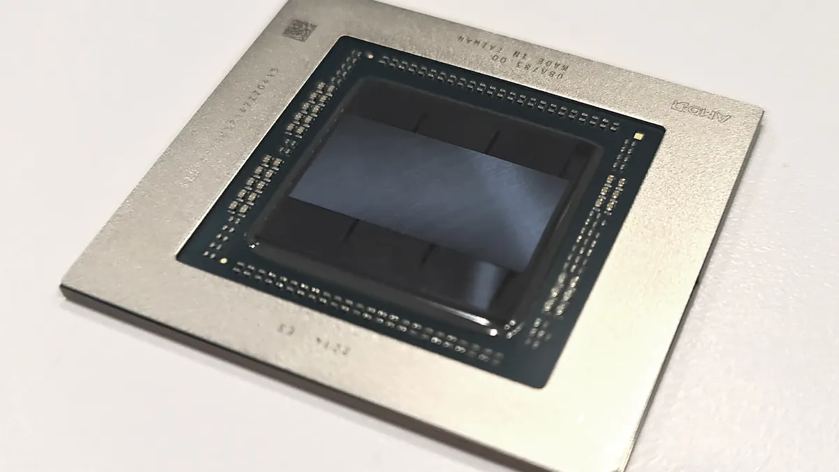
That's where AMD's using what's called an MCD. This takes all the stuff usually stuck surrounding the Graphics Engine—the Infinity Cache and the GDDR6 memory interfaces—and boots them off to their own chiplet. Each MCD is much, much smaller than the GCD, but therein lies one of the benefits of this chiplet system.
Whereas the Navi 21 GPU found in the RX 6950 XT is 520mm2, and the AD102 GPU in Nvidia's RTX 4090 is a whopping 608mm2, AMD's GCD for Navi 31 is just 300mm2.
Each MCD is only 37mm2.
A lower chip size makes for higher yields. Higher yields should make for a much better supply picture.
"The smaller the die, the better the yield, and so it is, just from an economic standpoint, those are all very small, very, very good yield," Laura Smith, corporate vice president, Graphics MNC and Product Management, tells me.
"If you put them all into one big die, then you'll see, and you see it in all sorts of products, you need some redundant capabilities, because you're going to have fallout."

I'd love to think this chiplet approach would have a desirable effect on the overall supply picture and thus trickle down to impact the prices and supply us gamers will actually see over at retailers after the initial launch fervour. A single chiplet that dramatically reduces die size while also being utilised across multiple products in AMD's lineup could be a real winner in that regard, even if AMD isn't targeting Nvidia's top GPU in performance. It certainly worked for Ryzen, which employed a similar approach with its cIOD—a die that brought together all the uncore functionality of the processor under one roof and on an older process node.
The same point can be made for AMD's RDNA 3 chips in regards to process nodes. The memory interface and the Infinity Cache weren't set to benefit a whole lot from TSMC's 5nm process node, so splitting them off from the core and manufacturing them on the cheaper 6nm node made more sense.
"When we are looking at chiplet design, we want to maximise it, which means we want to put the things that shrink well and get the benefits from the advanced and expensive technology nodes in that technology and the things that don't get much benefit we can leave behind on old technology nodes," Naffziger says.
"The right technology, the right job."


Best gaming PC: The top pre-built machines from the pros
Best gaming laptop: Perfect notebooks for mobile gaming
Naffziger worked on AMD's Ryzen chiplet approach—it was his "baby" for years—so it only makes sense that he'd be the one to think up the new way this technology could be applied to a gaming GPU. That also necessitated a new interconnect—GPUs are suckers for bandwidth—and that's where AMD's exciting Infinity Links comes in.
But to think this all started on a scrap of paper in a hotel during a boring meeting. So think about that next time you're sitting in a meeting listening to someone drone on about why your company has to turn off all the heating in the office this winter—you could dream up your next big breakthrough right there and then.