


The world of semiconductor manufacturing is an opaque one. Enthusiasts understand what a CPU is and what it does, but the actual steps and processes involved in their manufacture is far less understood by anyone that doesn't hold an advanced engineering degree or two. So, when Intel invited me to visit its facilities in Penang, Malaysia to learn more about chipmaking wizardry, I was more than happy to accept.
Broadly speaking, Intel's Malaysian facilities include areas that cut and sort incoming wafers, assemble and install them onto substrates before they take their final forms. At all stages there are tests and more tests before they're tested further. We were also invited to visit labs that analyze failed dies and chips, and even one that builds testing equipment for Intel factories all over the world. Additionally, there's a lab that tests the test equipment.
One of the Intel representatives I spoke with called it the most advanced manufacturing on the planet and it's hard to argue with that. Of course, you have stuff like quantum computers or fusion reactors at the cutting edge of scientific research, but they're not at the manufacturing stage.

And anyway, all of the R&D that goes into those things needs everything from laptops to supercomputers. And that means they need chips like those that pass through facilities like the ones in Malaysia. It's important work. Without chips and transistors, everything effectively grinds to a halt.
The technology, science, research and development, engineering, and frankly, wizardry of it all can seem otherworldly.
On a personal level, I find semiconductor manufacturing absolutely fascinating. The technology, science, research and development, engineering, and frankly, wizardry of it all can seem otherworldly. I am thankful for the chance to take a peek behind the curtain and gain an understanding of what goes into these magical little bits of technology.
The tour was made up of two parts. Well, three really. The first day of the tour consisted of visit to Intel's Penang Assembly and Test facility (PGAT). The name gives away its purpose. This facility takes the incoming dies and mounts them onto their PCB substrates, before thermal interface material or solder is applied, followed by heat spreaders. The second day involved a trip to the Malaysian mainland for a visit to Kulim based die sort and die pre facilities.
For this article, I mostly split it up according to the manufacturing stage rather than chronologically. We weren't allow to record anything or even carry a notebook in many places, so I hope my brain cache didn't fail.
Intel lays outs an aggressive roadmap

As part of the tour Intel laid out its vision and plans for the next few years. It refers to its plan as IDM 2.0 (Integrated Device Manufacturer). Having dropped the ball with its overly ambitious 10nm rollout followed by the pandemic fallout, the company has certainly needed a reset.

That means building sustainable, resilient supply chains and adopting manufacturing processes that scale effectively. Then there's the use of external foundries where appropriate and the introduction of Intel Foundry Services, where Intel's manufacturing expertise can be accessed by fabless customers.
A lot of that sounds a bit PR friendly but it's clear Intel has been executing this strategy for some time. Just look at how much money it's investing into various sites around the world, wooing clients, and striving to catch up to TSMC for manufacturing leadership.

Intel's aggressive goal is to achieve five nodes in four years. Intel 7 is in full production already, while Intel 4 (used by Meteor Lake) is ramping up. Intel 3 is then an evolution of Intel 4, while Intel 20A and 18A are planned to be ready for manufacturing in 2024. That means we're getting close to the angstrom era, with sub 1nm (10A) manufacturing already being developed.
With the amount of money being thrown around, plus a dose of protectionism from governments, I wouldn't bet against Intel catching up to TSMC sooner rather than later.
Oh, have you heard of AI? It's a thing apparently. Intel is betting on an open ecosystem and eventually sees AI becoming democratized and a ubiquitous part of not just cloud and LLM applications, but a part of everyday computing.
Wafers go under the knife, and sorting operations

Intel's Kulim facilities are located on the Malaysian mainland. This is where incoming wafers are processed, prepared and sorted before being sent off to assembly facilities around the world.
The Kulim facility houses a system integration and manufacturing facility. It produces testing equipment and boards for Intel fabs, factories and labs worldwide. In essence, it’s a facility for building and testing test equipment.
Location: Kulim, Malaysia
Opened: 1995
Purpose: High volume die preparation and sorting
Consumers processors sorted here: 12th and 13th Gen Core processors, Meteor Lake
Intel's Malaysia facilities don't include a wafer fabrication plant. The wafers are shipped to Malaysia from any of the various fabs in the USA, Ireland, or Israel. For an insight into what happens in a fab, it's well worth checking out Jacob's article, written after a visit to Intel's Israel plants last year.
The wafers arrive in what Intel calls the KMDSDP, or Kulim Die Sort Die Prep plant. Typical 300mm wafers are progressively cut up via a process that includes laser scribing and mechanical cutting with diamond saw blades. It sounds fairly rudimentary but even this is done with absolute precision. From there, the dies are moved onto sorting operations.

Once the wafers have been cut, the dies run though tests to determine what they will end up as. To use 13th Gen Rocket Lake chips as an example, the dies need to be tested and sorted to determine whether a particular die will end up as an i9 13900, 13900K or 13900KS.
The machines that do this sorting are amazing pieces of tech by themselves. There are row after row of them. Each weighs 1000 pounds. They are a bit like hovercraft, sitting on a cushion of air for easy movement, should a unit require maintenance. We saw one being easily pushed around with a lifter mechanism, handled by just two people.

Each die is tested by connecting it to a probe card which contains thousands of needles thinner than a human hair. Once the chips are tested, then they move onto the PGAT assembly and test factory before they take the form of the chips we know and love.
Behind every good die is a good substrate

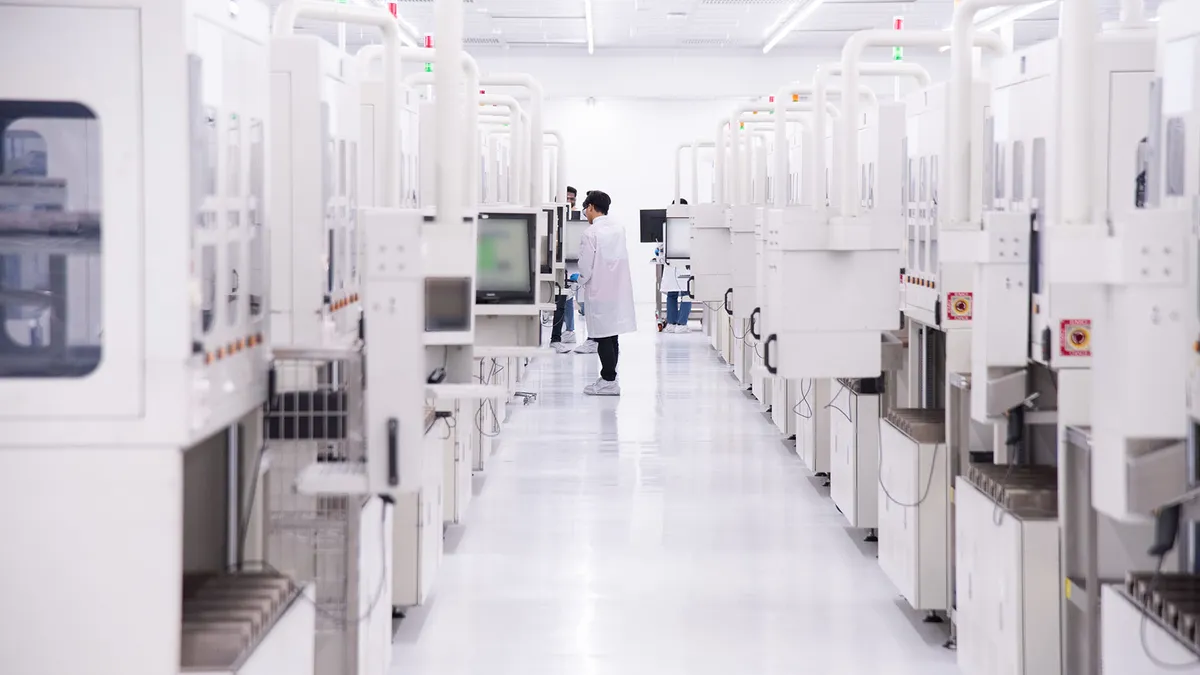
In order to access this part of the Intel Penang Assembly and Test facility (PGAT), we were required to suit up in order to conform to clean room requirements. One of these vast clean rooms houses machinery that installs incoming dies onto their substrates.
Location: Penang, Malaysia
Opened: 1972
Purpose: High volume chip assembly and testing
Consumers processors assembled here: 12th and 13th Gen Core processors, Meteor Lake
It used to be that monolithic dies could be slapped onto a substrate and that was pretty much that, but with modern chiplet designs, (or tiles in Intel parlance) the assembly process is much more complicated. Start adding 3D stacking and Intel's Foveros technology into the mix, and assembly is an obviously critical part of the chip making process.
Just take a look at an Intel Ponte Vecchio compute GPU below. It's perhaps the most ambitious processor in Intel's history. It packs in 47(!) tiles, five different process nodes and over 100 billion transistors onto one substrate.
When we talk about chip tech, we often refer to lithography and nodes, but chip packaging deserves just as much spotlighting, and that goes for AMD too with its Zen chiplet designs. Taking all of these tiles, with a mix of nodes and even manufacturers, getting them to talk to each other while maintain signal integrity, at scale and with all of its functionality intact is a massive achievement. Well done Intel.

Once the chips are attached to their substrates, they have an epoxy material applied. This ensures the dies are 100% level, ensuring physical stresses are uniformly distributed across the dies. In the picture above you can see Ponte Vecchio chips with and without the epoxy applied.
The chips are then sent off to settle for a while before the thermal interface material or solder is attached, and the heat spreader is installed (where applicable). They are then sent off for barrages of tests.

The PGAT facility houses design and development labs, a failure analysis lab and areas for testing chips in various stages of production, including tests that incorporate typical end user workloads.
Now, let's see what you little blighters can do.

The assembled chips are sent off to a part of the PGAT factory to confirm whether assembly was successful. First up is a burn in test. Machines punish the chips with high temperatures of over 100°C and voltages up to the limits of the specification.
Following the burn-in test, a series of electrical tests are performed, this involves tests of the functionality of the chip and a check to ensure the traces and substrate are functioning as they should.

If that's successful, the chips move onto real world testing. Chips are mounted onto testing platforms that begin to resemble something like the PC we know and love. These in-house-built test platforms use different operating systems and software to mimic real world use. I saw 3DMark looping on a series of systems. I half expected to see an engineer playing Baldur's Gate 3. For research and testing purposes, of course!
Failure analysis. Yep, there's a sonar test.

As much as Intel would like it to be the case, not every chip comes out of the factory in perfect working order. That doesn't mean the failed ones are completely dead though. Maybe testing reveals an anomaly, a functionality failure, or something that requires analysis. In that case, they are sent over to Intel's failure analysis lab.
This lab is a bit smaller than the vast floor spaces common to the rest of the facility, but it's no less cool. Intel has all kinds of advanced equipment to test for failures. There's the obvious visual inspections via microscopes or electrical tests with oscilloscopes, but there's more advanced thermal imaging equipment too.
One of the most interesting things of a whole tour was seeing a kind of ultrasonic sonar wave testing machine that involves sitting the chip in water.

Now is a good time to mention that we weren't allowed to take pictures inside any of these facilities, and in fact were not allowed to carry phones, watches, or wallets.
And I'm kicking myself for not seeing this first hand, but apparently there was at least one Battlemage GPU out in the open in this lab. This is a next generation Intel GPU, and it's a good sign that these are in the production stage and being analyzed. It would indicate Intel's next gen graphics card range is absolutely on target for a 2024 launch.
Well, so long as the failures aren't too grand in scale.
Testing equipment, and the testing of the test equipment that does the testing
Factories like this need a lot of custom equipment. The machines used for manufacturing and production are finely calibrated pieces of precision equipment. It's not the kind of stuff you can pop in a box and send back to whoever made it.
Intel has a division it calls System Integration and Manufacturing Services (SIMS). Its purpose is to make equipment for testing and validating the chips at many stages of the process. All of the post assembly test rigs such as the one seen below are made in house.
There's even a section of the plan that tests the test equipment. In case you didn’t know, there's a lot of testing of everything!

A couple of examples of Intel's bespoke test equipment include machines that perform burn in stress testing while another performs backend testing. The picture below shows a custom machine used to test power related components. I recall the PCB being massive and very thick. You can just see how thick it is on the right in the pic below. I shudder to think what each of these would be worth.

Some random observations and closing thoughts
As I began writing this up, I wished I'd been allowed to carry a notebook. Not so I could pass trade secrets to AMD, but just so I could remember the massive amounts of information we were given!
But apart from that, the trip was amazing. As a reviewer, this kind of insight into the manufacturing process was invaluable, personally and professionally. I like to think I understand CPUs pretty damn well, but seeing the sheer scale of Intel's operation was a real eye opener.
The picture below shows one of the many semi autonomous robots that scoot around the die sorting and prep area. It put out a constant appealing musical chime. They take various dies or wafers from one area of the factory to another, always with a smile!

I like to think I understand CPUs pretty damn well, but seeing the sheer scale of Intel's operation was a real eye opener.
Arthur C. Clarke is remembered for his three 'laws'. The third of which states: "Any sufficiently advanced technology is indistinguishable from magic".
Those inside Intel would say it's all advanced engineering, and they're right, honestly. But after seeing what these folks do first hand, there has to be a little bit of magic involved, surely. If not that, then I'll go with aliens.