AMD’s Polaris Shoots for the Stars

More FinFETs
Getting back to the FinFET discussion, if we leave the world of GPUs behind, we’ve seen evidence of 20nm scaling issues elsewhere as well. Smartphones and tablets showed some tremendous performance improvements when they moved from 40nm to 28nm, giving us improved performance and battery life. The move from 28nm to 20nm on the other hand was far less impressive. The good news is that smartphones and tablets frequently don’t run heavy workloads, so things like power gating and voltage islands helped…but under load, when the transistors are active, leakage is still an issue. That’s perhaps one of the reasons why 20nm SoCs in smartphones have had more problems with overheating than earlier models.

That brings us to FinFET, and what it does to fix the leakage problem. The original idea came in 1989, by Hisamoto, who called it the “Delta FET” because it looked a bit like a delta wing. The name FinFET caught on in 2000 when UC Berkeley did some additional work on the idea, referring to the “wing” as a “fin” instead. The fin part of the name comes from the fin-like structure that rises above the substrate, which the transistor gate wraps around, giving far more surface area and control over the gate.
The first production FinFET devices came in 2012, when Intel rolled out Ivy Bridge with their 22nm FinFET process. It’s more difficult to manufacture FinFET than planar transistors, but the tradeoff between cost and performance eventually made it a requirement. Just like AMD and Intel (and others) moved from aluminum to copper-based transistors about ten years back in an effort to reduce leakage and improve performance—and added SOI, or Silicon on Insulator as an added bonus—FinFET is the way forward for sub-20nm process technology.

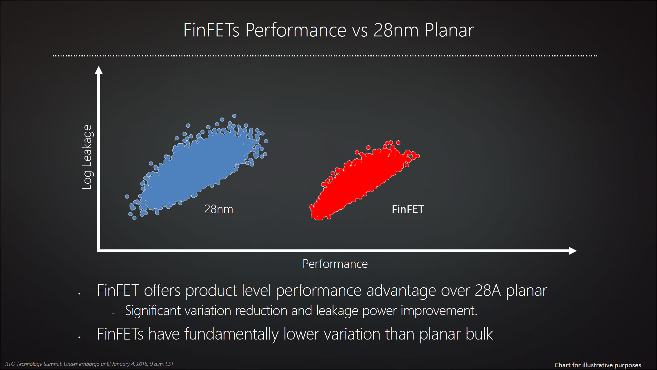
RTG also presented the above slide, showing that not only does FinFET allow for improved performance, but it also reduces the variation among transistors. There’s still variation, of course, but a processor can only run as fast as its weakest link—the top-left corner of each “blob” in the slide. So if you can decrease the leakage range and improve the minimum clock speed, you end up with a faster chip.

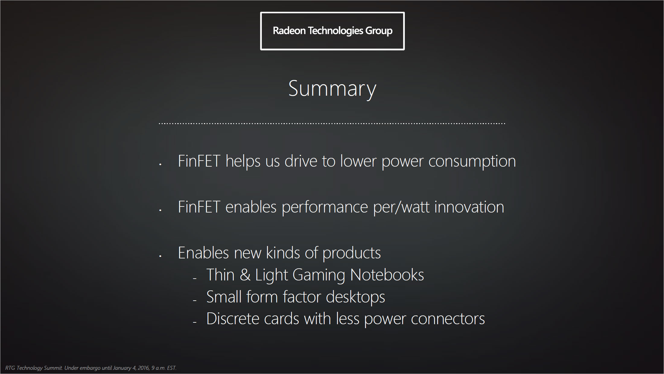
Overall, FinFET ends up being a tremendous benefit to processor designers. It allows for a reduction in power—or more performance at the same power, thanks to the performance per watt improvements. This will allow for GPUs that are more power friendly, including even thinner and lighter gaming notebooks. Or it can be used to make a mainstream GPU that doesn’t require any extra power connectors (e.g., the GTX 750 Ti). Or a chip can include even more cores than before and provide better performance. RTG mentioned around a 2X improvement in perf/watt at one point, which potentially means a doubling of performance on the fastest parts; we’ll have to wait and see if we get that big of a boost, but it’s at least possible.
Keep up to date with the most important stories and the best deals, as picked by the PC Gamer team.
Jarred's love of computers dates back to the dark ages when his dad brought home a DOS 2.3 PC and he left his C-64 behind. He eventually built his first custom PC in 1990 with a 286 12MHz, only to discover it was already woefully outdated when Wing Commander was released a few months later. He holds a BS in Computer Science from Brigham Young University and has been working as a tech journalist since 2004, writing for AnandTech, Maximum PC, and PC Gamer. From the first S3 Virge '3D decelerators' to today's GPUs, Jarred keeps up with all the latest graphics trends and is the one to ask about game performance.


