A Brief History of CPUs: 31 Awesome Years of x86
AMD Athlon XP
Still part of the Athlon family, AMD's XP revision would add SSE instructions and represent a more aggressive approach to marketing. XP stood for eXtreme Performance and tied in nicely with Microsoft's Windows XP operating system, but it didn't stop there. AMD also went back to using a Performance Rating (PR) system for labeling its processors. Officially, AMD's PR rating (yes, we realize that's redundant) was used to denote an XP chip's performance to that of an equivalent Thunderbird core, so an AMD Athlon XP 1800+ would, in theory, offer the same performance as a Thunderbird running at 1.8GHz (1,800MHz). However, in practice it was much more widely used as a point of reference next to Intel's Pentium processor, even if this was incorrect, leading many to refer to the abbreviation as a Pentium Rating.
Yet another revision -- the Thoroughbred, or T-Bred -- would be released and drop the manufacturing process down from 180nm to 130nm. Later models would also increase the frontside bus from 100MHz (Thunderbird) and 133MHz (XP) to 166MHz (T-Bred).
But the most popular Socket A Athlon was the one built around the Barton core. Barton chips first appeared in 2003 and represented a tremendous value for enthusiasts and overclockers alike. Of particular interest were early revision Barton 2500+ processors, which shipped with an unlocked multiplier. By upping the multiplier, most Barton 2500+ chips could easily be transformed into AMD's flagship 3200+ model. Not only were Barton CPUs affordable, but so were the high-end motherboards they ran on, namely the Asus A7N8X Deluxe and Abit NF7-S Rev2, the two top overclocking boards of the time. When AMD began locking the multiplier, these and other top-end boards allowed the 2500+ to run like a 3200+ with a quick frontside bus adjustment.
From a technical standpoint, the Barton core doubled up its L2 cache to 512KB and increased the number of transistors from around 37 million (depending on the core) to 54.3 million.
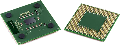
Date Released: 2001
Clockspeed: 650MHz - 2.25GHz
Did you know?
AMD Sempron
Picking up where the Duron left off, AMD's Sempron brand replaced the Duron as the company's budget chip and Celeron competitor. And like the Duron, Semprons featured reduced L2 cache, or at least most of them did. Standing as an oddity among the rest was the Sempron 3000+ Not much more than a name change at first, early Semprons were basically Athlon XP chips with some of its cache disabled. However, the Sempron 3000+ contained 512KB of L2 cache and ran at 2.0GHz with at 166MHz frontside bus. For all intents and purposes, the Sempron 3000+ was really a Barton 2700+, if such a chip existed. It contained the same amount of L2 cache as a Barton, ran the same speed frontside bus, and was clocked between a Barton 2600+ (1.9MHz) and 2800+ (2.08GHz).
Semprons would continue to evolve alongside (and under) AMD's mainstream processor lines and still exist today.
Keep up to date with the most important stories and the best deals, as picked by the PC Gamer team.
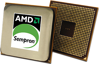
Date Released: 2004
Clockspeed: 1.4GHz to 2.3GHz
Did you know?
AMD Athlon 64
If you're an AMD loyalist, you may want to skip this section, as it's like remembering an old friend before he was later gunned down. AMD's highest point came with with release of its Athlon 64 series, the first 64-bit processors aimed at mainstream users. While Intel was busy trying to ramp up its NetBurst-based P4 processors, AMD stole the performance crown with a much more efficient architecture and an integrated memory controller.
Not without some intial growing pains, A64 was first made available for Socket 754 motherboards, which lacked dual-channel memory support, and Socket 940, a server-oriented socket requiring buffered RAM. But like a perfect storm, Socket 939 brought with it dual-channel memory support, PCI-E, and a long-term upgrade path that helped cement AMD as the performance leader.
Even though A64 offered native 64-bit support, it was also fully backwards compatible with 32-bit code without any noticeable performance penalty. This was huge for Windows users, who were still living in a 32-bit world (the same holds true today, although 64-bit Vista is lightyears ahead of 64-bit XP).
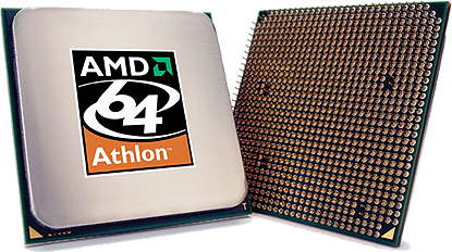
Date Released: 2004
Clockspeed: 1.0GHz to 3.2GHz
Did you know?
Intel Pentium D
The ill-fated NetBurst architecture made its last stand in Intel's Pentium D brand. Pentium D processors consisted of two single-core CPU dies fused to a multi-chip module. While not as elegant as AMD's dual-core design, the Pentium D offered decent multitasking performance, good overclocking performance, and comparatively low prices. The Pentium D provided a solid alternative to the Intel faithful who refused to invest in AMD.
Date Released : 2005
Clockspeed: 2.66GHz to 3.73GHz
Did you know?
AMD Athlon 64 X2
Continuing its dominance on the desktop, AMD's Athlon 64 X2 series consisted of two CPU cores on a single die sharing a crossbar that connects them to the integrated memory controller. These internal data links paid huge performance dividends compared to Intel's dual-core configuration, which had each core pushing communication through a shared frontside bus. SSE3 instructions were added to the X2 series, but most importanly, AMD managed to keep the new chip on Socket 939. While not all boards were compatible, many 939 mobos could handle an X2 upgrade with nothing more than a BIOS update, which meant AMD could tap into an existing install based for its new processors.
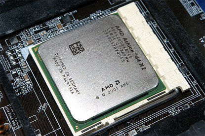
(Image Credit: Flickr Fr3d.org)
Date Released: 2006
Clockspeed: 1.0GHz to 3.2GHz
Did you know?
The Athlon 64 4000+ was the last single core model in the Athlon 64 series, but single-core Athlons lived on in the FX line.
Intel Core 2
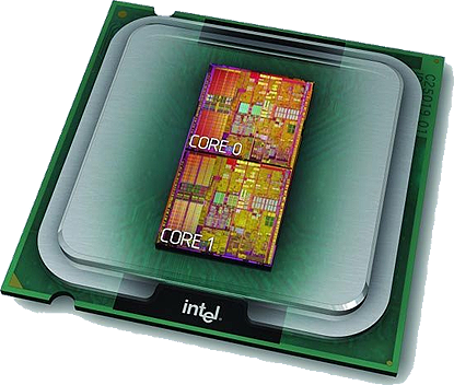
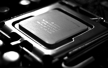
Waking out of its Netburst slumber, Intel took the CPU world by storm with its Core 2 architecture. Instead of remaining fixated on higher clockspeeds, Intel refocused its attention on being more efficient with its pipeline. This meant a return to lower clockspeeds, however it also meant a return to prominence as the performance king. After Prescott failed to live up to its hype, the media remained cautiously optimistic that Core 2 could live up to Intel's promised performance gains, but much to the chagrin of AMD, Core 2 lived up to its billing, and then some.
The first Core 2 Duos burst out of the gates with 167 million transistors, a 65nm manufacturing process, 2MB of L2 cache, and a 1,066MHz frontside bus. Despite debuting at just 1.86GHz and 2.13GHz (E6300 and E6400, respectively), Core 2's performance made it instantly attractive, and Intel's aggressive pricing sealed the deal.
Later on, Core 2 would move to a 45nm manufacturing process with its Penryn revision, pack up to 820 million transistors into a quad-core package, and reach as high as 3.2GHz.
(Image Credit: Flickr BodHack)
Date Released : 2006
Clockspeed: 1.8GHz - 3.2GHz
Did you know?
Intel actually made single-core Core 2 chips for its mobile line, based on the Merom and Penryn designs.

