Nvidia Pascal P100 architecture deep dive
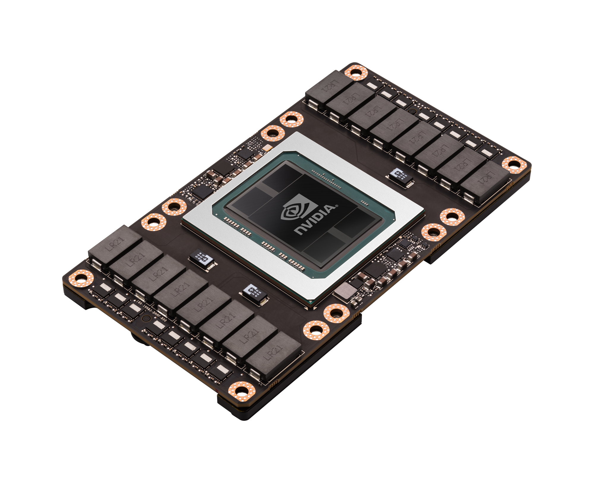
Lars Nyland is a senior architect at Nvidia, and Mark Harris is a chief technologist for GPU computing software. They took turns discussing the Tesla P100, starting with the above high-level overview. Pascal is Nvidia's highest performance compute architecture ever, regardless of what type of workload you're running. This is an important distinction, as for example the Maxwell architecture was severely lacking in FP64 performance.
In some ways, Pascal is similar to the Fermi architecture, which was the last time Nvidia offered FP64 performance running at half the FP32 rate; Kepler dropped to 1/3 performance on FP64 while Maxwell was limited to only 1/32 FLOPS rate on FP64. For workloads that don't need the extra precision, Maxwell was fine, but many scientific applications stuck with Tesla K40/K80 (K110B GPUs) for this reason while others were able to move to the Tesla M40 to take advantage of its superior FP32 performance. With Tesla P100, all workloads will run optimally on a single architecture.
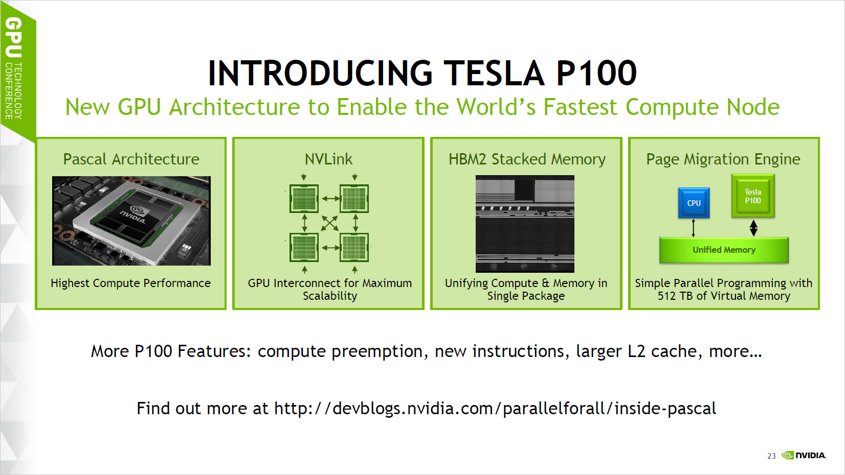
Along with the improvements to the raw performance, Pascal brings several other technologies that will help with compute. NVLink improves inter-processor communication, relieving the PCI Express bus of this burden and providing much higher throughput for enhanced scalability. The Tesla P100 will also use HBM2 (High Bandwidth Memory), similar to AMD's Fiji architecture but with significantly more capacity. Finally, Nvidia has added a Page Migration Engine, which combined with unified memory allows the addressing of up to 512TB of virtual memory.
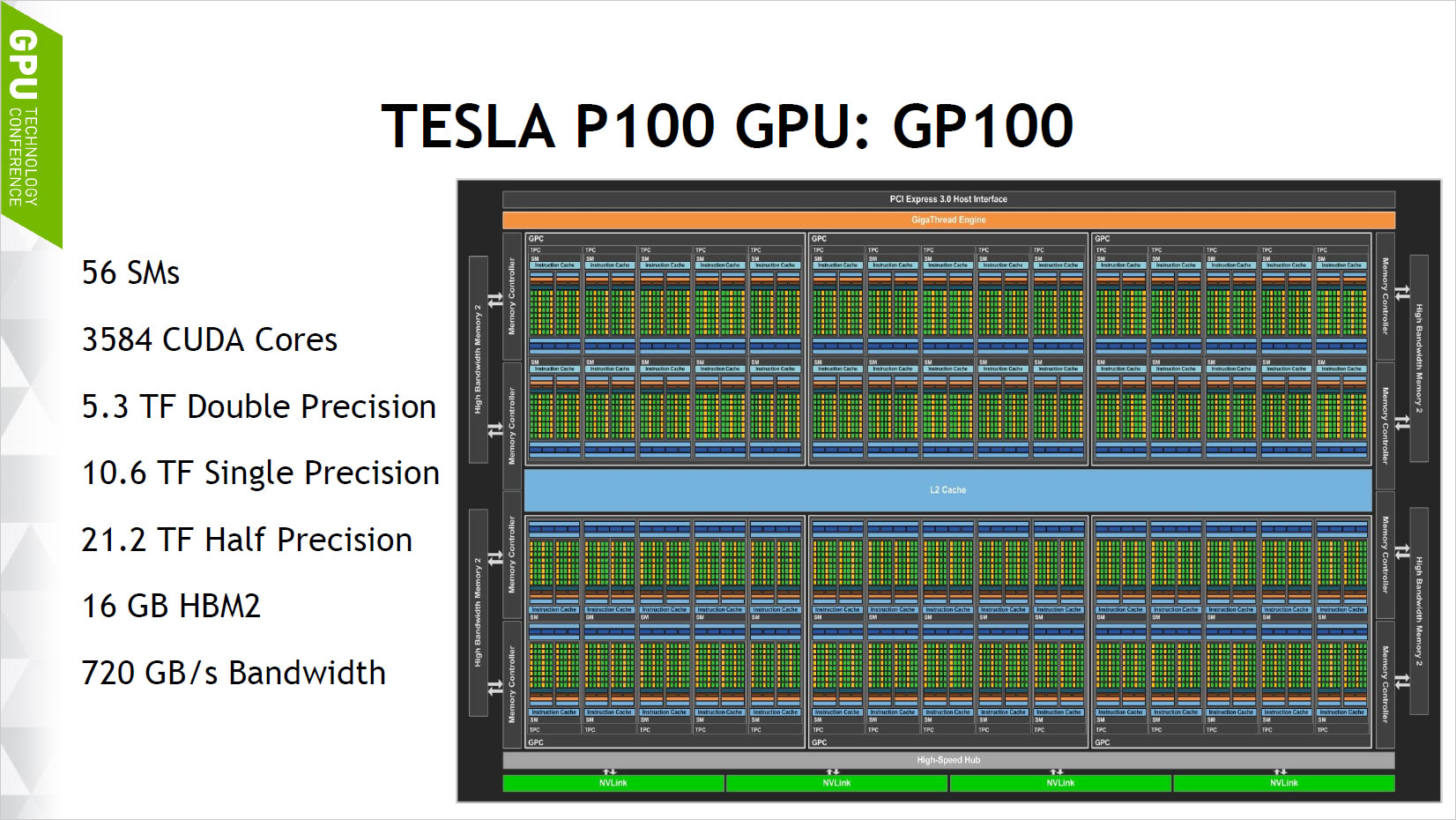
The block level diagram of Pascal shows many of the key changes that have occurred. One thing worth pointing out here is that this presentation is the only place so far where we've seen Nvidia refer to the GPU as the GP100—whether this was a mistake or intentional isn't clear, but it does indicate that Tesla P100 is likely to use the same core as future Quadro and perhaps even high-end GeForce devices. From a high level view, GP100 has six functional blocks of 10 SMs each, but four of the SMs are disabled to give a total of 56 active SMs.
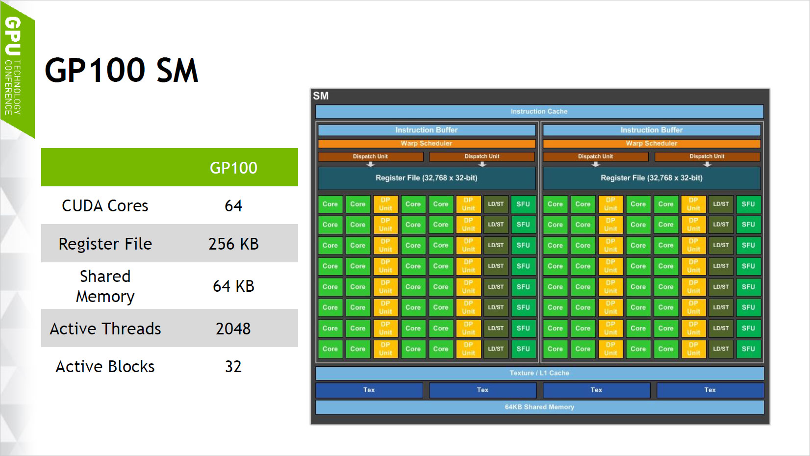
Looking at an individual SM, there are 64 CUDA cores, and each SM has a 256K register file, which is four times the size of the shared L2 cache size. In total, the GP100 has 14,336K of register file space. Compared to Maxwell, each core in Pascal has twice as many registers, 1.33 times more shared memory, twice the shared memory bandwidth, and twice the number of warps. (Or if you prefer, another way of looking at it is that each SM has the same register file space, but half as many cores in Pascal compared to Maxwell.) These changes help Pascal to improve instruction throughput and improve efficiency. We mentioned earlier the improved FP64 (double-precision floating point) performance of Pascal compared to Maxwell, but Pascal also adds support for half-precision FP16 running at twice the rate of FP32, which is new for Nvidia's hardware. Here's the specifications comparison looking at the Tesla P100, M40, and K40:
| Tesla Products | Tesla P100 | Tesla M40 | Tesla K40 |
|---|---|---|---|
| GPU | GP100 (Pascal) | GM200 (Maxwell) | GK110 (Kepler) |
| SMs | 56 | 24 | 15 |
| TPCs | 28 | 24 | 15 |
| FP32 Cores / SM | 64 | 128 | 192 |
| FP32 Cores / GPU | 3584 | 3072 | 2880 |
| FP64 Cores / SM | 32 | 4 | 64 |
| FP64 Cores / GPU | 1792 | 96 | 960 |
| Base Clock | 1328MHz | 948MHz | 745MHz |
| GPU Boost Clock | 1480MHz | 1114MHz | 810/875MHz |
| Peak FP16 GFLOPs | 21,217 | 6,844 | 5,040 |
| Peak FP32 GFLOPs | 10,609 | 6,844 | 5,040 |
| Peak FP64 GFLOPs | 5,304 | 213 | 1,680 |
| Texture Units | 224 | 192 | 240 |
| Memory Interface | 4096-bit HBM2 | 384-bit GDDR5 | 384-bit GDDR5 |
| Memory Size | 16GB | 12GB/24GB | 12GB |
| L2 Cache Size | 4096KB | 3072KB | 1536KB |
| Register File Size / SM | 256KB | 256KB | 256KB |
| Register File Size / GPU | 14336KB | 6144KB | 3840KB |
| TDP | 300 Watts | 250 Watts | 235 Watts |
| Transistors | 15.3 billion | 8 billion | 7.1 billion |
| GPU Die Size | 610mm² | 601mm² | 551mm² |
| Process | 16nm FinFET | 28nm | 28nm |
In terms of peak throughput (the 21 TFLOPS number Nvidia has bandied about), GP100 does best with FP16. K40 and M40 only support FP32 or FP64, and in those workloads the difference isn't quite as large, though P100 is still around 50 percent faster than M40 and nearly 150 percent faster than K40. For FP64, meanwhile, P100 is more than 20 times faster than M40, and a sizeable 3.8X jump in performance over K40. Memory bandwidth is also greatly improved thanks to HBM2, with GP100 getting 2.5 times as much bandwidth. Finally, outside of the recently launched 24GB Tesla M40, the P100 also has more memory than the previous Tesla offerings.
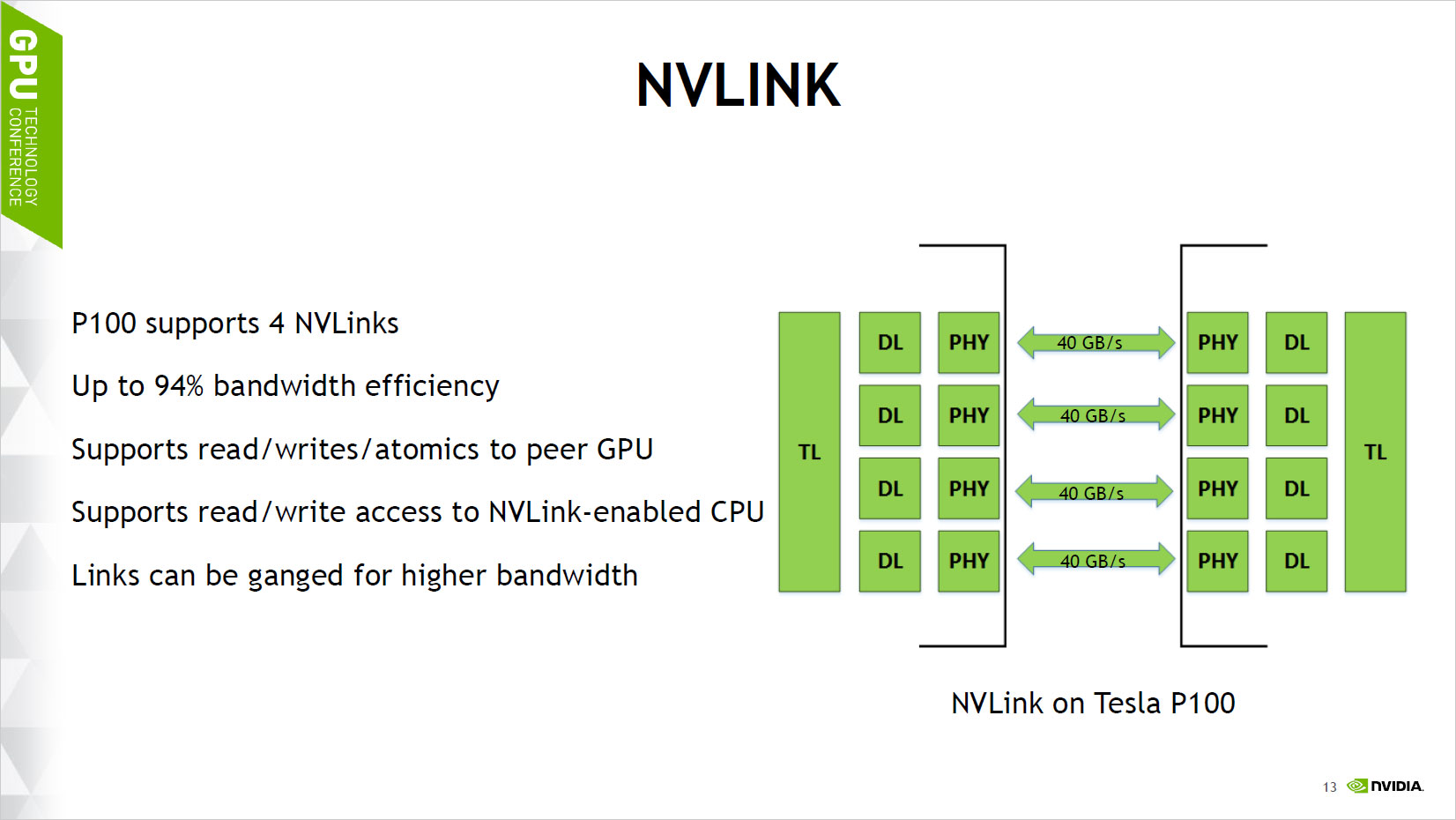
Moving on, each P100 will support up to four NVLinks to either other P100 GPUs, or to a CPU. Unified memory allows each GPU to directly access the memory from another GPU as well, though obviously the 40GB/s NVLink speed could be a bottleneck in some scenarios. It's still 2.5 times as fast as sending data over the PCIe bus, however, with less chance of other traffic getting in the way.
Keep up to date with the most important stories and the best deals, as picked by the PC Gamer team.
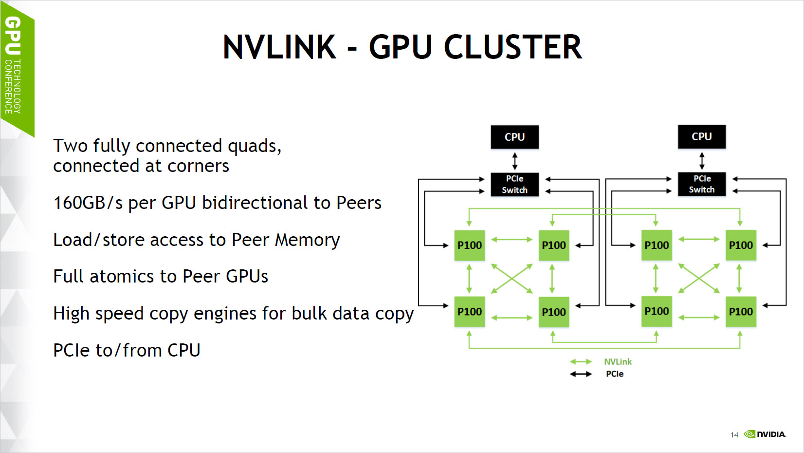
At present, Nvidia supports up to eight Tesla P100 GPUs in a cluster, using the above topology. In this arrangement, all GPUs are either one or two hops away, and the same goes for the CPUs.
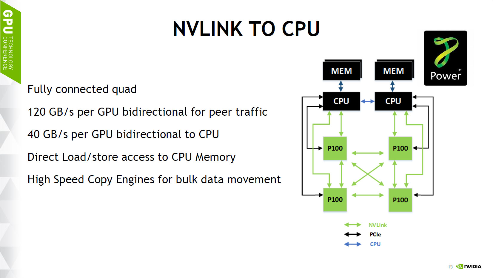
IBM is also planning on supporting NVLink for CPU communications, in which case one of the links for each GPU in a quad GPU configuration can be utilized for GPU-to-CPU communications.
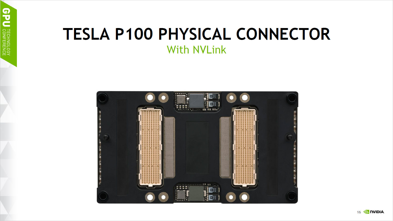
This is what the back of the Tesla P100 module with NVLink looks like. And here's something super important to consider when talking about Tesla P100: at present, the P100 will only be sold as a complete solution (e.g., the DGX-1 server), because it uses a new SXM2 mezzanine connector; there are currently no PCIe-based variants of the P100, though they're "being investigated." Obviously we'll see PCIe Quadro and GeForce graphics cards with Pascal at some point in the future, but Tesla is taking a break from PCIe for now. IBM also has an upcoming POWER8 server with support for NVLink connectors, though availability hasn't been announced.
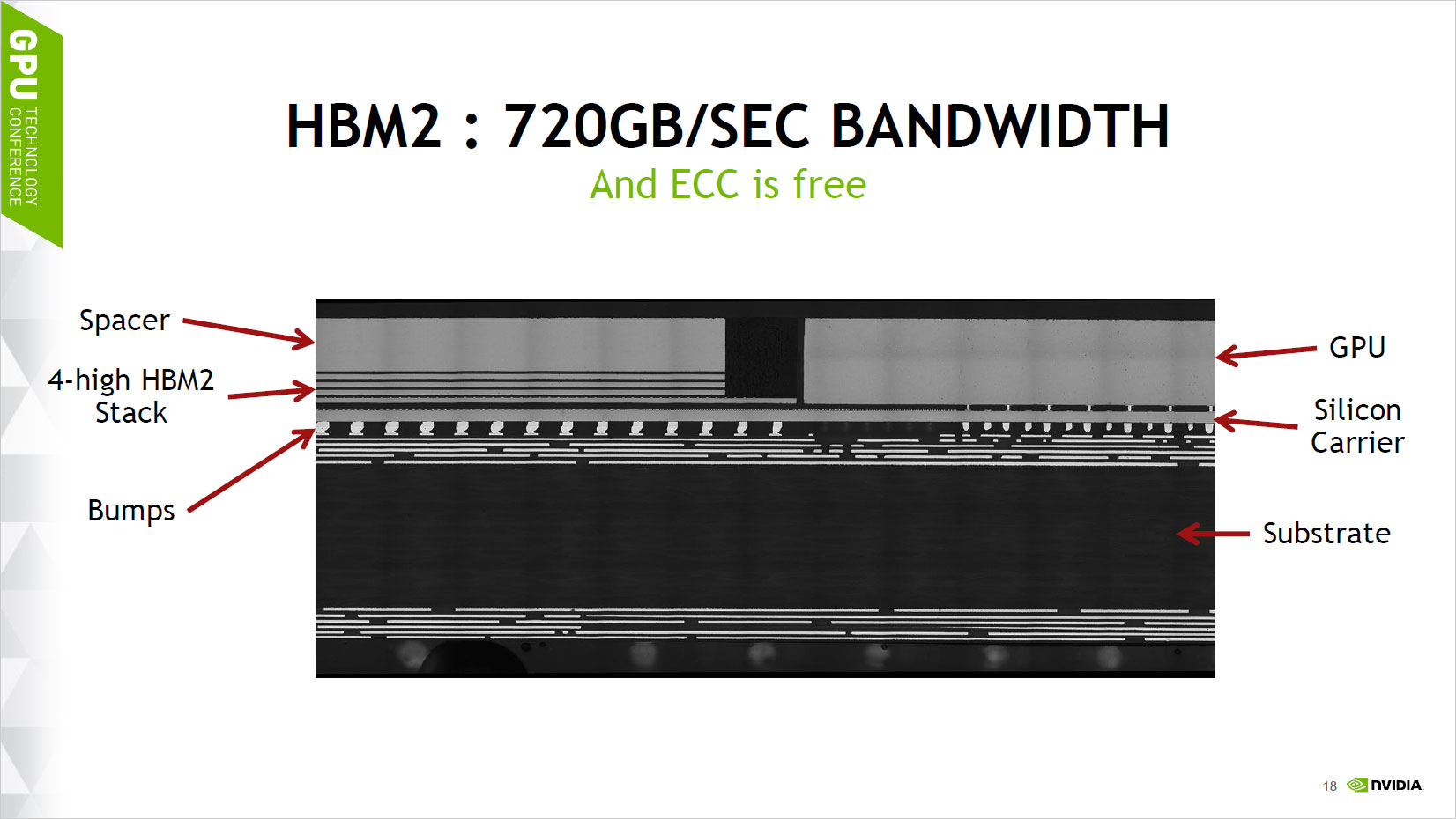
There's not a lot more to say about HBM2. Fundamentally, it's a similar design to HBM1, only capacity per layer is substantially higher. The bus width is still 1024-bit per stack, but instead of a 1GHz clock, HBM2 is running at 1.4GHz, yielding 720GB/s of bandwidth. One of the benefits for designs like Tesla P100 and Quadro is that ECC is built into HBM2, so no extra work needs to be done in that regard. HBM2 could conceivably go as high as 32GB in four stacks (using eight layers per stack), but for now Nvidia is using four layers. All designs that use HBM need a silicon interposer, basically a large but somewhat simplistic chip that routes signals between the GPU and the HBM modules, and this helps to make the overall package + memory area much smaller than traditional GPU designs.
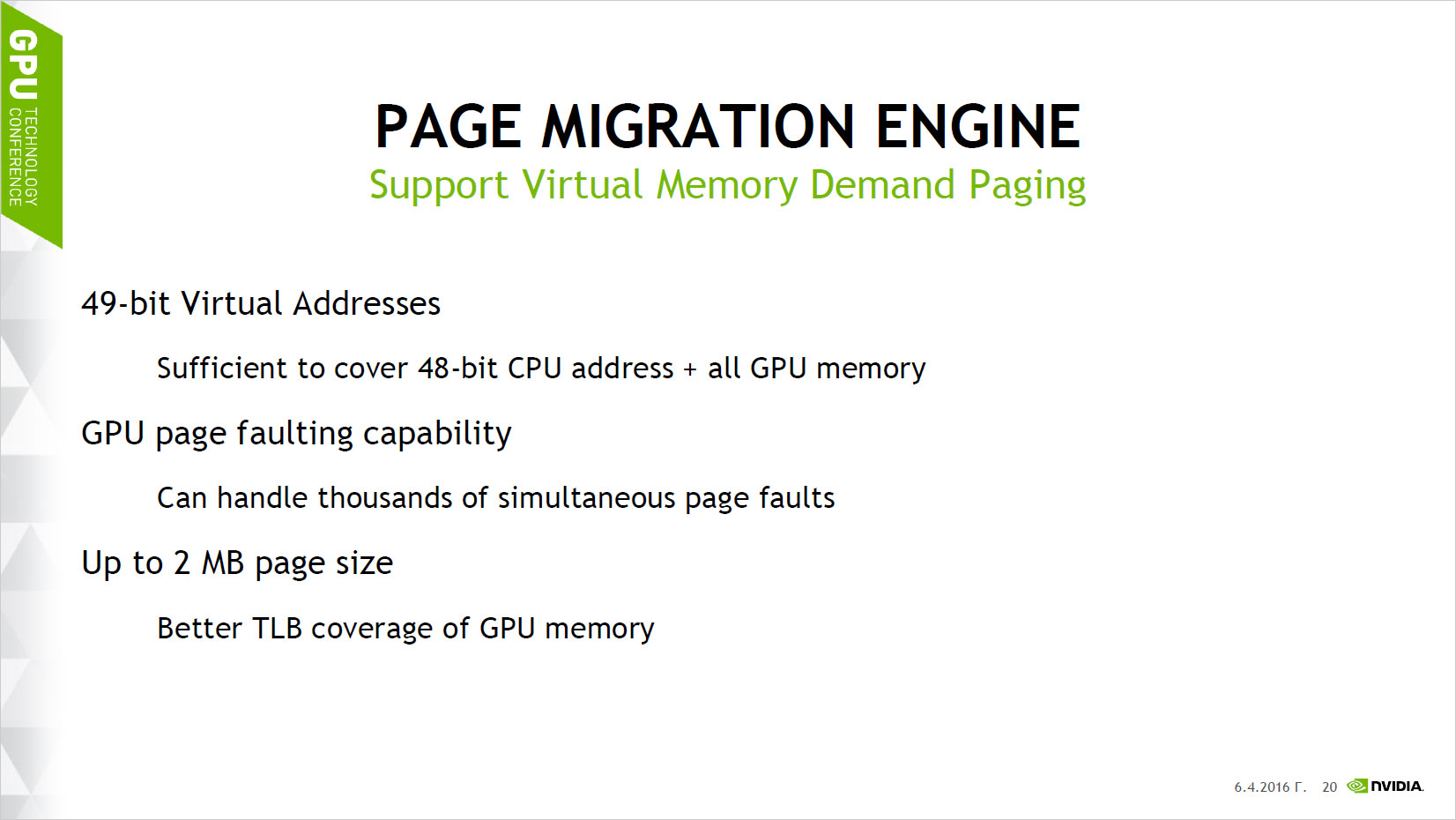
Along with unified memory, one of the big changes with Pascal is the inclusion of a Page Migration Engine. This provides several benefits, one being the ability of the GPU to handle page faulting—it will automatically request the needed data if it's not present, and it can coalesce multiple overlapping requests at the same time. If a program is running and tries to access data stored in a memory page, it might generate a whole bunch of page faults while the data is retrieved. However, once the page is loaded, all of those page faults can clear at the same time.
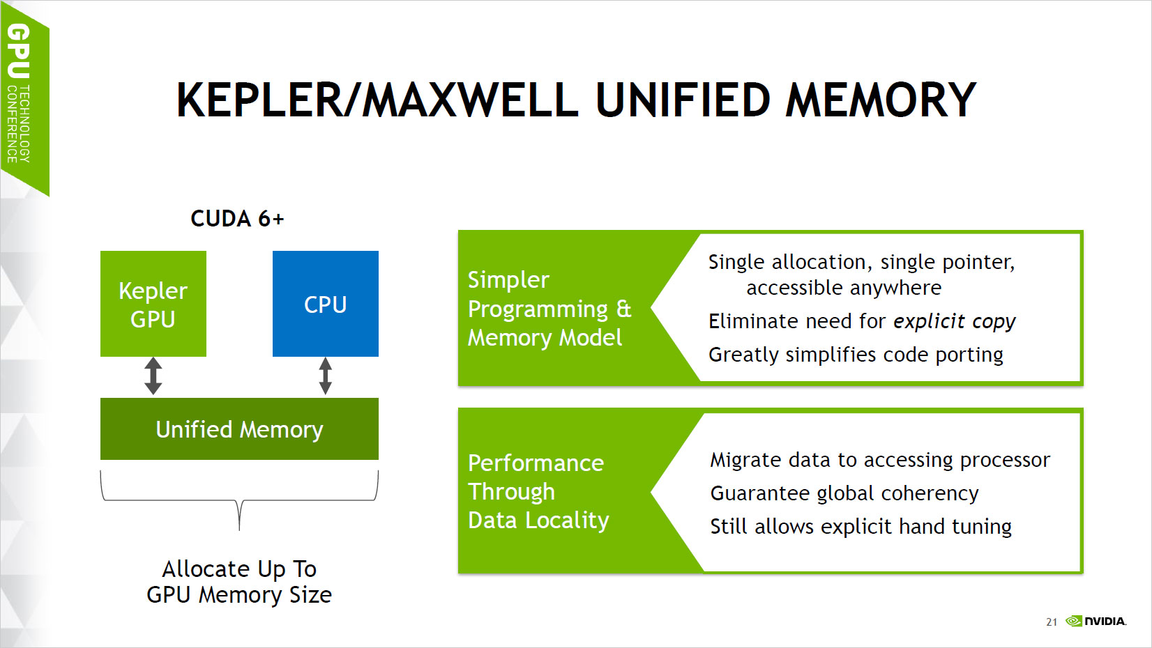
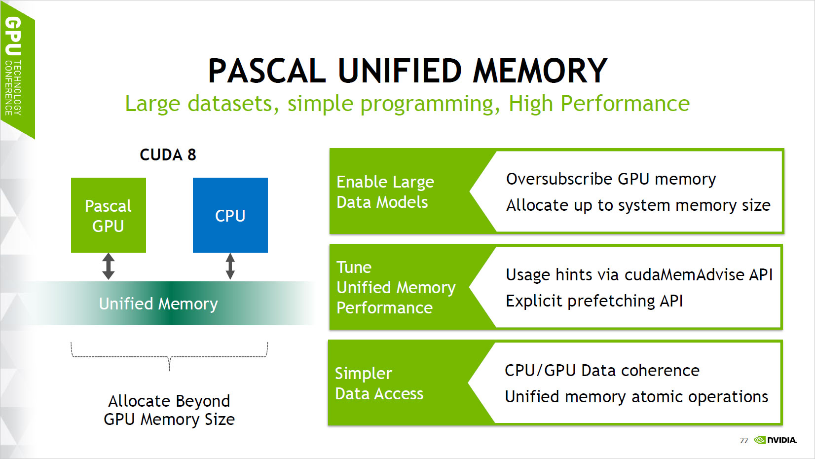
These two slides show the differences between how Maxwell/Kepler handled unified memory compared to Pascal. Pascal allows for allocating substantially more memory than your GPU has, and it lets the Page Migration Engine sort things out. While it's still possible to hand-tune memory requests to improve performance, it makes working with data from multiple sources—system, local, or another GPU—much easier.
Finally, there are other elements of the Pascal architecture that weren't really covered in much detail. One of these is particularly interesting, however: compute preemption. With Pascal, Nvidia has added the ability to preempt at the instruction level, so it's possible to switch tasks at any time to run a different workload. This could be beneficial for things like VR and asynchronous time warp, but it also allows better GPU sharing on servers and in the cloud. That could be useful for things like GeForce Now, where at present GPUs are allocated to subscribers on a 1-to-1 basis; with Pascal GPUs it would potentially become easier to run multiple games on each GPU, though obviously the need to store the registry file, cache, and other state variables every time you preempt means you don't want to do it very often.
From the compute perspective, Pascal and GP100 are shaping up to be a large jump in performance, just as we expected from the move to 16nm FinFET. It will be interesting to see how much of what has been revealed here applies to other Pascal offerings, as GP100 at least clearly has some features that are unnecessary in client workloads (e.g. FP64, ECC, virtual memory). Will all Pascal designs use 64 CUDA cores per SM, or could we see a split where other GPUs drop some of the FP64 units in order to reduce the die size or add additional cores? That doesn't seem likely, but stranger things have happened.
Jarred's love of computers dates back to the dark ages when his dad brought home a DOS 2.3 PC and he left his C-64 behind. He eventually built his first custom PC in 1990 with a 286 12MHz, only to discover it was already woefully outdated when Wing Commander was released a few months later. He holds a BS in Computer Science from Brigham Young University and has been working as a tech journalist since 2004, writing for AnandTech, Maximum PC, and PC Gamer. From the first S3 Virge '3D decelerators' to today's GPUs, Jarred keeps up with all the latest graphics trends and is the one to ask about game performance.

