TSMC touts a 6-nanometer manufacturing process as AMD settles into 7nm
TSMC anticipates 6nm being used for GPUs, high-performance computing, and other products.

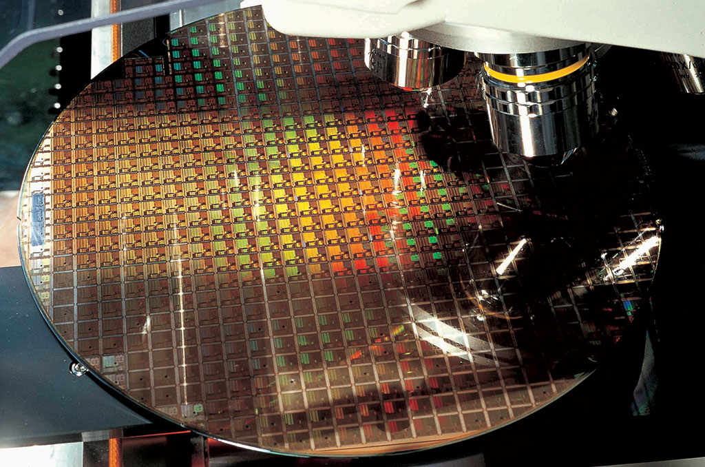
The dust never has time to settle in tech, and if we're talking about semiconductors and chip fabs, dust is a bad thing—it's one of the reasons you see pictures of engineers in full body suits, otherwise known as a cleanroom suit. We're not here to talk about engineering garb, though. Instead, let's discuss TSMC's unveiling of a 6-nanometer manufacturing process.
TSMC's announcement comes hot on the heels of Samsung announcing both a tape out of its own 6nm lithography, and development of 5nm FinFET, which is now ready for sampling to customers.
What's interesting about TSMC's announcement is that it too is already working on 5nm. In fact, 5nm is in what's called the risk production phase, which basically means there could be issues that need tweaked, but it is available. 6nm is scheduled for risk production in the first quarter of 2020.
So what's the point of 6nm, if TSMC is already on to 5nm? That's a good question, and I have two potential answers which are sort of related to one another. Let's start with the first one.
TSMC's 6nm node doesn't require new equipment. It's a "direct migration from N7-based designs."
"Its design rules are fully compatible with TSMC’s proven N7 technology, allowing its comprehensive design ecosystem to be reused. As a result, it offers a seamless migration path with a fast design cycle time with very limited engineering resources for customers to achieve the product benefits from the new technology offering," TSMC explains.
The benefit for customers is that N6 (6nm) delivers 18 percent higher logic density over N7 (first-gen 7nm), allowing for designs that pack more transistors into the same space for potentially better performance and lower power consumption. So on the surface, the point of N6 is to give TSMC's customers a rather affordable upgrade path over 7nm.
Keep up to date with the most important stories and the best deals, as picked by the PC Gamer team.
That's answer No. 1. The second potential answer is marketing. There are no hard and fast rules for naming process nodes—Intel's 10nm, for example, is roughly equivalent to TSMC's 7nm. It's possible that TSMC's 6nm node is just tweaks to its 7nm+ (N7+) node. Like N7+, which is what AMD's Zen 2 (Ryzen 3000) is based on, the new N6 node utilizes new capabilities in extreme ultraviolet (EUV) lithography (as opposed to N7's deep ultraviolet, or DUV, lithography).
If that's the case, TSMC could have just called this 7nm++ (N7++), as it's basically 7nm with a higher transistor density. But hey, 6nm sounds better. And maybe TSMC learned a thing or two about marketing numbers after the 16nm to 12nm transition.
In any event, TSMC anticipates its 6nm node being used in range of applications, from GPUs and high-performance computing, to artificial intelligence and 5G infrastructures, and more.
The mere existence of TSMC's N6 alongside N7 and N5 points yet again to how difficult it's becoming to shrink our microprocessor manufacturing technologies. As transistors get smaller, a single set of rules won't necessarily deliver the best results. That's likely at least part of the reason for the multiple simultaneous options being offered by TSMC, Samsung, GlobalFoundries, and Intel.
Paul has been playing PC games and raking his knuckles on computer hardware since the Commodore 64. He does not have any tattoos, but thinks it would be cool to get one that reads LOAD"*",8,1. In his off time, he rides motorcycles and wrestles alligators (only one of those is true).


