The AMD Ryzen 7: plenty of power, but underwhelming gaming performance
Great for video editors, not so great for gamers.

Ryzen's architecture
From a high level, Zen looks a lot like Intel's Core architecture. Gone is the CMT module and in its place AMD has a 4-core/8-thread SMT (symmetric multi-threading) building block. (Intel's Hyper-Threading is basically a trademarked name for SMT, incidentally.) AMD said that Ryzen gets more of a benefit from SMT than Intel gets from Hyper-Threading, with gains of around 40 percent with SMT enabled compared to 25 percent on Intel.
These blocks can be partially disabled, so there are also 6-core/12-thread parts coming, but those are Ryzen 5 parts slated for Q2 (May/June) and not today; Ryzen 5 will also have 4-core/8-thread models. Later on in Q3, AMD will also have 4-core/4-thread Ryzen 3 CPUs, including APUs based on Ryzen. There could potentially be even lower tier 2-core/4-thread parts at some point. AMD hasn't talked about going below 4-core publicly, but Ryzen is intended to scale from ultra-low-power through high-end desktop and on to server parts, so a dual-core ultramobile part at some point seems likely.

I'm always a sucker for die shots, and along with the high-level overview of Ryzen, AMD also provided the above image that zooms in on a single core, pointing out the various structures. There are four of these cores, along with 8MB of L3 cache, in each Ryzen 'module.' The size of the complete module is apparently 44mm^2, with the L3 cache using 16mm^2. This compares favorably with Intel's 4-core/8-thread size, which has an area of around 49mm^2. Size doesn't necessarily equate to performance, but it again illustrates how AMD's Ryzen is similar in a variety of ways to Intel's offerings.

Along with SMT support, the pipeline and various other elements of the architecture have also been reworked. The L1 cache is a faster write-back design, and compared to Excavator and the earlier Bulldozer family parts, L2 cache delivers up to twice the bandwidth and L3 cache is up to five times the bandwidth. There's a new micro-op cache, which can eliminate a lot of power hungry decoding for cache hits, and each core can issue up to six micro-ops (or four fp-ops) per cycle—similar to Skylake's 6-wide issue width and 50 percent higher than the 4-wide design of the Bulldozer family of CPUs.

Zen has an improved 'perceptron' branch prediction algorithm, now decoupled from the fetch stage, which also helps performance. And not to downplay these aspects, but Zen also features larger load, store, and retire buffers, along with improved clock gating. One thing we don't know is how many pipeline stages there are. There will be some stages like fetch and decode that take place before the micro-op cache, while the rest of the pipeline follows. I've heard guesses of 18-20 stages, with four coming before the micro-op cache, but those could be completely wrong.
One aspect of Zen that AMD's particular proud of is the new Infinity Fabric, which defines the interconnects and protocols for a variety of data traffic. AMD talked about this at its previous Tech Summit in December, explaining that with the separate Jaguar and Bulldozer families of processors, not to mention graphics chips, there were many different interconnects and protocols being used. It basically took a lot of extra time and effort to get things working. The Infinity Fabric unifies all of these items under a large umbrella, and while the specific implementations can vary (eg, Hyper Transport, PCIe, point-to-point, etc.), the protocols are all well-defined. Vega GPUs will also include the Infinity Fabric.
It's hard to overstate how big of a fundamental change all of this represents, and it means everything we know about AMD's CPU performance from the past may no longer apply. AMD had a performance target of 40 percent better IPC with Zen versus Bulldozer (Excavator), and not only did AMD hit that mark, but in general IPC is even higher. The 'worst' improvement in IPC that AMD measured is around 52 percent, with some workloads showing 70 percent or better IPC. All these architecture changes should provide some excellent per-clock performance improvements, and with Ryzen clocking at up to 4.0GHz, it should be competitive with Intel's Broadwell-E processors.
Keep up to date with the most important stories and the best deals, as picked by the PC Gamer team.

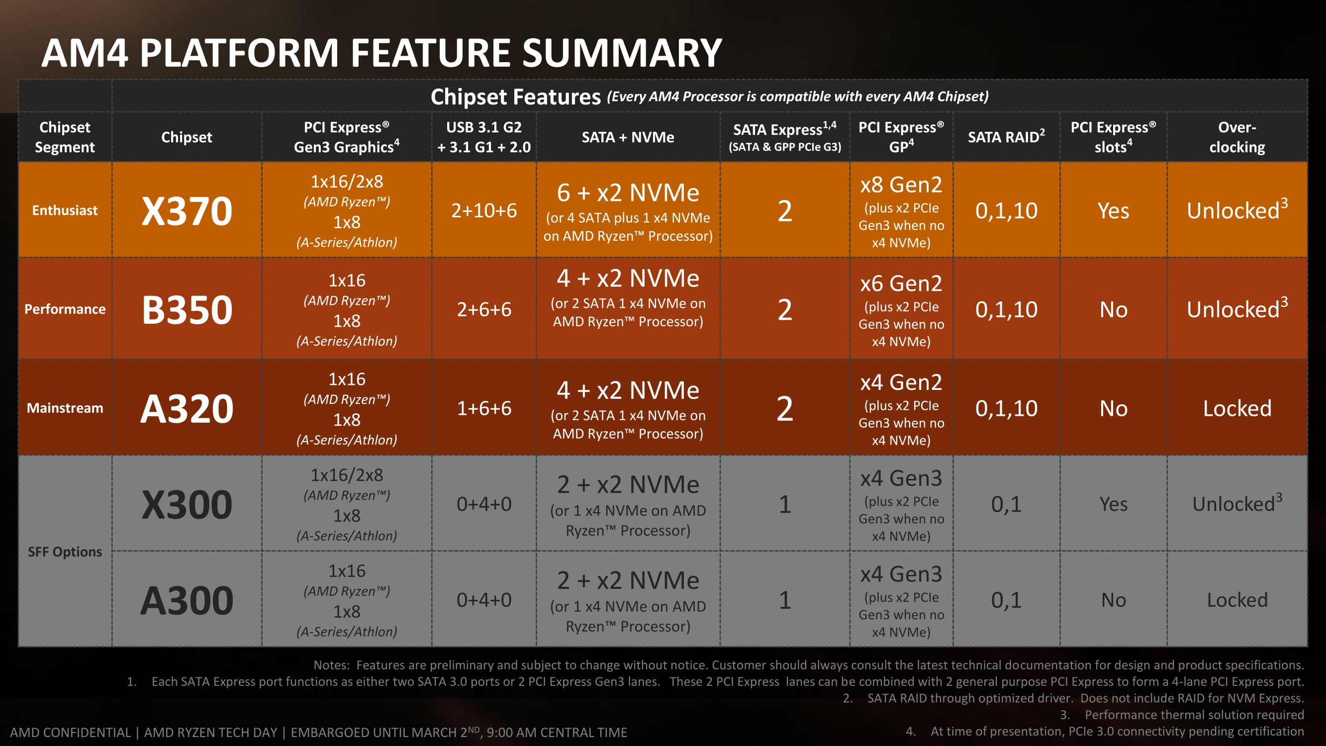
Then there's the platform. Zen will use a new AM4 socket, with one of several chipsets, A320, B350, and X370. Regardless of chipset, the platform will remain as a dual-channel DDR4 setup, and the CPU socket has 1331 pins. Ryzen has multiple PCIe lanes available for connecting to external devices. 16 lanes will go to the GPU slot, with a splitter allowing two x16 slots running at x8 connections. Another four lanes are available for an M.2 NVMe x4 slot. The high-end X370 chipset supports two USB3.1 10Gbps ports, 10 USB3.0 ports, and six USB 2.0 ports. Sticking with dual-channel makes sense as well, as it keeps motherboard costs in check, and it allows for up to 64GB max memory.
AMD also has overclocking support on three of the chipsets, the X370, B350, and X300—only the A320 and A300 lack support for overclocking. The X300 and B350 will be more economically priced, and AMD says we should see motherboards that support overclocking starting at around $100. The Ryzen 7 parts are expensive and I'd recommend going the X370 route for the 8-core CPUs, but when Ryzen 5 arrives, it could really shake up the mainstream market.
Jarred's love of computers dates back to the dark ages when his dad brought home a DOS 2.3 PC and he left his C-64 behind. He eventually built his first custom PC in 1990 with a 286 12MHz, only to discover it was already woefully outdated when Wing Commander was released a few months later. He holds a BS in Computer Science from Brigham Young University and has been working as a tech journalist since 2004, writing for AnandTech, Maximum PC, and PC Gamer. From the first S3 Virge '3D decelerators' to today's GPUs, Jarred keeps up with all the latest graphics trends and is the one to ask about game performance.


