Join The Club


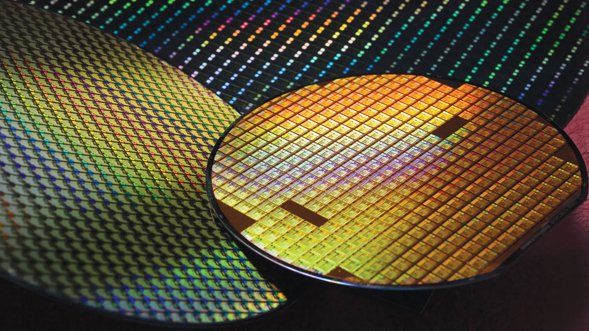
Every now and then, I come across a tech development that makes me feel like I'm living in the future, and this is one of those moments. A team of scientists at Fudan University in Shanghai have published a study detailing their latest achievement, a fully functional memory chip built with integrated 2D materials a few atoms thick. Yesssss. This is the Star Trek-level technology I was promised as a child.
Well, maybe that's jumping the gun a bit. Still, the achievement here is incredibly impressive (via Tom's Hardware). Essentially, the researcher's new Atom2chip process allowed them to flow a layer of molybdenum disulphide, functioning as a memory array, on top of a 0.13 micrometre CMOS silicon chip—fusing together an emerging atomic-scale, "2D" technology with traditional methods to create a working hybrid memory chip.
Article continues below 
The end result of this incredibly clever method is a memory chip with a five megahertz peak operating speed but an incredibly low power draw, with each bit said to consume just 0.644 picojoules of juice. Not only that, but the process appears to result in a very stable output, with a reported success rate of 94.34%. A mass-manufacturing method in waiting, then? Perhaps.
Up until now, two-dimensional materials have been demonstrated in individual lab experiments, not in working components that could potentially scale to meet demand. And as our conventional chip production methods become ever more difficult as the processes become smaller and smaller, 2D materials might be the key to stretching Moore's Law all the way down to the atomic limit in the decades to come.
So, the upshot is, your CPU in the next few decades (I'm guessing here) might well make use of this very process in order to up the transistor density, all the while delivering massive power savings compared to the chips of today. Pie in the sky? Up until now, perhaps, but it's breakthroughs like this that could lead to it all becoming a reality.
Now, where's my Starship Enterprise? Still under development? Fine. Denser, more power-efficient chips thanks to nanoscale tech within my lifetime, though? Sure, I'll take it.
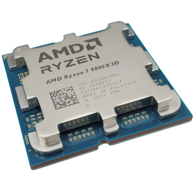
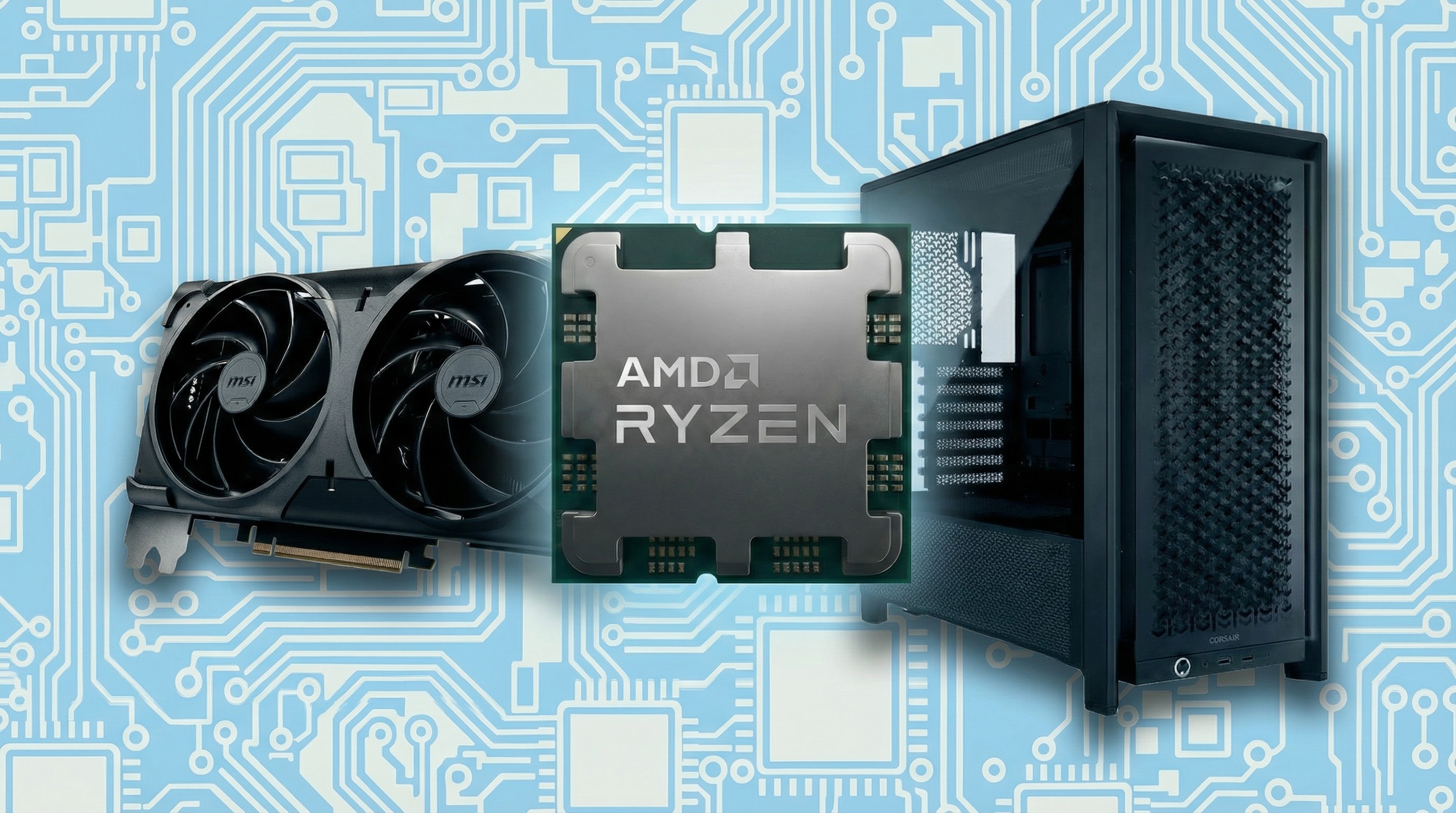
1. Best CPU: AMD Ryzen 7 9800X3D
2. Best motherboard: MSI MAG X870 Tomahawk WiFi
3. Best RAM: G.Skill Trident Z5 RGB 32 GB DDR5-7200
4. Best SSD: WD_Black SN7100
5. Best graphics card: AMD Radeon RX 9070

You must confirm your public display name before commenting
Please logout and then login again, you will then be prompted to enter your display name.