SK Hynix is touting '4D' NAND flash memory that isn't really 4D
Marketing gone wild.

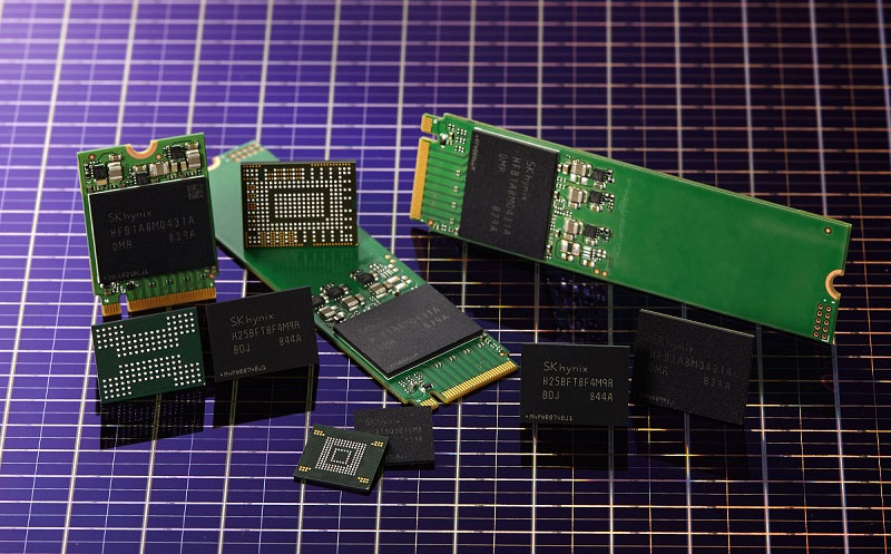
SK Hynix on Sunday launched what it is billing as the "world's first 96-layer 512Gb (gigabit) CTF-based 4D (four dimensional) NAND flash" memory, or 4D NAND for short. That's a mouthful, but it's the 4D NAND that is the attention grabber and needs further explaining.
The introduction of 3D NAND technology was a big deal in the memory space. By stacking layers of NAND cells, memory makers could pack more memory into tighter spaces, and save money in the process. It was a win-win.
SK Hynix's 4D NAND nomenclature suggests a fourth dimension, but that's not actually the case. The new chips are based on triple-level cell (TLC) arrays and pair a couple of technologies to further improve density, and purportedly performance.
Our friends at TomsHardware broke this down quite nicely back in August when SK Hynix first introduced the concept of 4D NAND technology. SK Hynix's solution is built on what's called a CTF (charge trap flash) design, just as Samsung, Toshiba, and Western Digital. It's not a new technology by any stretch.
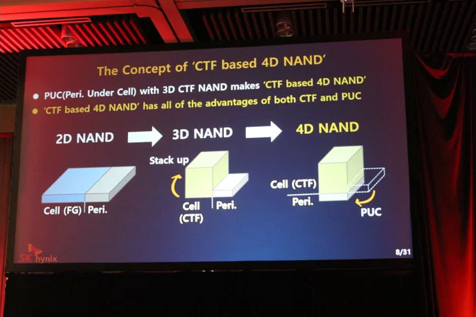
What is new is SK Hynix's pairing of its CTF design with its periphery under cell (PUC) technology. What does that entail? There are two main parts to 3D NAND flash—the array and periphery circuitry. The array consists of vertically stacked layers of NAND cells to store data, and the periphery circuitry sits next to the stacks.

What SK Hynix has done is to move the PUC underneath the array, as shown in the image above, and call it 4D NAND. That's clever marketing, which SK Hynix alludes to in its press release.
"SK Hynix combined its 3D CTF with PUC for the first time in the industry, which is different from the way of integrating 3D floating gate and PUC. As a result, it attained the industry’s finest performance and productivity. The company named the product ‘CTF-based 4D NAND Flash’ to distinguish it from current 3D NAND flash technologies," SK Hynix said.
Keep up to date with the most important stories and the best deals, as picked by the PC Gamer team.
While it's not actually utilizing a fourth dimension, SK Hynix claims a 30 percent reduction in chip size and a 49 percent increase in bit productivity compared to its 72-layer 512Gb 3D NAND. It's also touting 30 percent higher writes and 25 percent higher read performance.
"Also, its data bandwidth is doubled to the industry’s biggest 64KB. With the introduction of a multiple gate insulators architecture, its data I/O speed reaches 1,200Mbps at 1.2V of operation power," SK Hynix added.
SK Hynix says its 4D NAND flash solution will go into mass production before the end of the year.
Paul has been playing PC games and raking his knuckles on computer hardware since the Commodore 64. He does not have any tattoos, but thinks it would be cool to get one that reads LOAD"*",8,1. In his off time, he rides motorcycles and wrestles alligators (only one of those is true).


