Intel's 18A 'hallelujah' moment is the biggest bet the company has ever made
Intel CEO doubles, triples, quadruples down on the company's road map

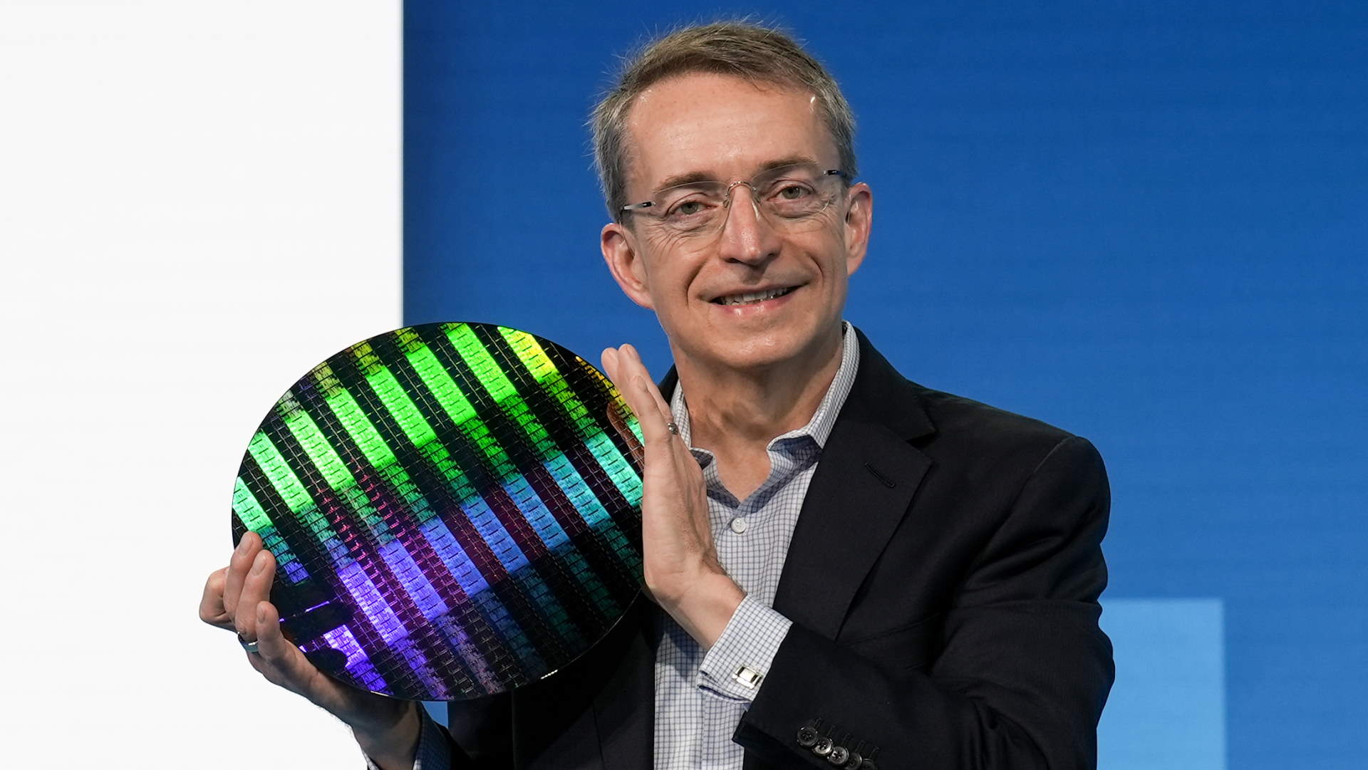
Despite Intel seemingly already struggling to stick to its latest round of radical roadmap promises, what with Meteor barely making its 2023 launch window, here comes CEO Pat Gelsinger sextupling down on the whole "five nodes in four years" thing and admitting that the culmination of that relentless schedule is the biggest bet the company has ever made.
In an interview with Stratechery, Gelsinger is speaking specifically of 18A, the production process that qualifies as number five in Intel's accelerated roadmap. Intel 7 we already have in Alder Lake and Raptor Lake CPUs, Intel 4 arrives at the end of the year with Meteor Lake, then's there's 20A and last and most definitely not least, it's 18A.
Asked if 18A is Intel betting the company, Gelsinger was remarkably unequivocal. "Betting the entire company? I don’t know that I’d go all that way, but this is the biggest bet we have ever made as a company because it also puts incredible stress on the financials of the company," he said, explaining that Intel is "racing through capital" as it chased its ambitious roadmap.
But why is 18A rather than any of the other landmarks along the way so important? Well, that's all about backside power or what Intel calls PowerVia, which in the simplest possible terms means supplying power to the transistors from below rather than above. Which kinda begs a "so what?" response. Well, here's what according to Gelsinger.
It comes down to the problems caused by feeding power down through the multiple layers of wiring and interconnects that sit on top of the transistors in a modern chip.
"When you look at a metal stack up and a modern process, leading edge technology might have fifteen to twenty metal layers. Metal one, metal two…and [then] the transistors down here. So it’s just an incredible skyscraper design. Well, the top level of metals is almost entirely used for power delivery, so now you have to take signals and weave them up through this lattice. And then you want big fat metals and why do you want them fat? So you get good RC characteristics, you don't get inductance, you're able to have low IR drop right across these big dies."
The problem? Those big power lines cause interference.
Keep up to date with the most important stories and the best deals, as picked by the PC Gamer team.
"They're screwing up your metal routing that you want for all of your signals. So the idea of taking them from the top and using wafer-level assembly and moving them to the bottom is magic, right? It really is one of those things, where the first time I saw this laid out, as a former chip designer, I was like, “Hallelujah!”, because now you're not struggling with a lot of the overall topology, die planning considerations, and you're going to get better metal characterization because now I can make them really fat, really big and right where I want them at the transistor, so this is really pretty powerful."
According to Gelsinger, the entire industry has suddenly woken up to the benefits of backside power and is racing to implement it in their future silicon, including the 800-pound gorilla of chip foundries that is TSMC. The thing is, as Gelsinger would have it at least, Intel has the jump on everyone else, and by several years.
"We are ahead by years over the industry for backside power or PowerVia. Everybody’s racing to get their version up and running, and we’re already well underway and in our second and third generation of innovation here," Gelsinger claims.
So, it's that core innovation which is set to not only put Intel's CPUs back on top in technological terms, but also drive customers to Intel as customers for its new foundry offering.

Best Black Friday PC gaming deals: All the best discounts in one place
How to avoid overpaying on a Black Friday gaming laptop deal: How much to pay, and where to buy from
How to spot the best Black Friday prebuilt deal: Don't pay over the odds for a PC this year
Indeed, Gelsinger actually mentions arch rival AMD when musing over Intel's approaches to potential foundry customers. But companies making Arm processors seem to be Intel's main ambition. "I want to be the best partner for Arm going forward. The majority of logic foundry wafers are Arm-based today," Gelsinger reckons.
Anywho, we'd normally say there's countless years to wait to see if a plan four node jumps down the road pans out. But no. Intel and Gelsinger have staked their reputation on delivering 18A and a return to leadership in 2025. Will Intel deliver? Who knows.
It'll be interesting to see how good those first Meteor Lake laptop chips are, that will be the first big test. Then there are Arrow Lake desktop CPUs due next year on Intel's 20A node, which will actually be the first Intel silicon with backside power. That's likely to be almost a test node for PowerVia, with the subsequent 18A node being the one that's going to go out to foundry customers.
The only problem is that this is all theoretical for now. We've yet to actually see any retail products that go beyond step one of Intel's bold multi-node roadmap. And time is running out.

Jeremy has been writing about technology and PCs since the 90nm Netburst era (Google it!) and enjoys nothing more than a serious dissertation on the finer points of monitor input lag and overshoot followed by a forensic examination of advanced lithography. Or maybe he just likes machines that go “ping!” He also has a thing for tennis and cars.

 Join The Club


