From Voodoo to GeForce: The Awesome History of 3D Graphics
Keep up to date with the most important stories and the best deals, as picked by the PC Gamer team.
You are now subscribed
Your newsletter sign-up was successful
Want to add more newsletters?
Join the club
Get full access to premium articles, exclusive features and a growing list of member rewards.
Nvidia GeForce 6 Series
Between running loud (in the beginning) and struggling to remain competitive with ATI's 9800 Series, the GeForce 5 architecture served as somewhat of an anomaly, one which was redeemed with the release of the GeForce 6 Series. GeForce 6 ushered in Shader Model 3.0 support, Nvidia's PureVideo technology, and multi-videocard support with SLI.
Comparing blueprints, GeForce 6 consisted of a larger die, almost twice as many transistors, a pixel fill rate nearly three times as high as the GeForce 5, and a four-fold increase in pixel pipelines (16 total). Later Nvidia would release its GeForce 6 Series in PCI-E form.
A card that proved popular among overclockers was the original 6800, sometimes referred to as the 6800nu (Non Ultra).These cards were built with the exact same chip as the 6800GT and Ultra, however 4 of its 16 pipelines came disabled. In some cases, these diasbled pipelines were actually defective, but overclockers quickly found out this was not always the case. Using an overclocking program called RivaTuner, it was possible to unlock the dormant pipelines, essentially transforming a vanilla 6800 into a faster performing (and pricier) 6800GT. And it was a low risk mod, too - if the the card displayed artifacts after applying the software mod, the original settings could easily be restored.
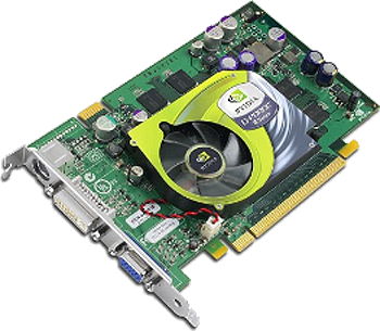
(Image Credit: Nvidia)
Model: GeForce 6600
Date Released: 2004
Interface: AGP/PCI-E
Shader Model: 3.0
DirectX: 9
Manufacturing Process: 0.11 micron
Core Clockspeed: 300MHz
Memory Clockspeed: 500MHz
Memory Bus: 128-bit
Transistors: 146 million
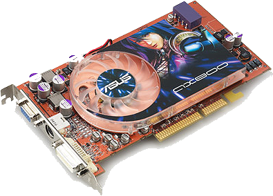
(Image Credit: techimo.com)
Model: GeForce 6800
Date Released: 2004
Interface: PCI-E
Shader Model: 3.0
DirectX: 9
Manufacturing Process: 0.13 micron
Core Clockspeed: 325MHz
Memory Clockspeed: 600MHz
Memory Bus: 256-bit
Transistors: 222 million
Keep up to date with the most important stories and the best deals, as picked by the PC Gamer team.
(Image Credit: hardwarezone.com)
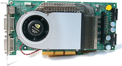
Model: GeForce 6800 Ultra Extreme
Date Released: 2004
Interface: PCI-E
Shader Model: 3.0
DirectX: 9
Manufacturing Process: 0.13 micron
Core Clockspeed: 450MHz
Memory Clockspeed: 1200MHz
Memory Bus: 256-bit
Transistors: 222 million
XGI / Trident XG40
When XGI Technology announced its Volari line of videocards in September of 2003, nobody knew what to expect. In fact, hardly anyone had even heard of XGI, who had emerged as a new graphics pision just four months prior. But XGI wasn't truly a new kid on the block. XGI, or e X treme G raphics I nnovation (see what they did there?), had previously existed as the Multimedia Product pision of Silicon integrated Systems (SiS). Not long after XGI branched off under its own moniker, the company went and acquired Trident's mobile graphics pision, which was responsible for developing a small handful of Volari videocards.
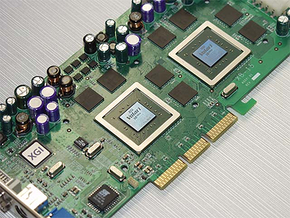
On the higher end of the Volari spectrum sat the XG40 chipset, which provided the foundation for the Volari V8 Ultra and Volari Duo V8 Ultra. The V8 Ultra utilized a 0.13 micron manufacturing processor, boasted 90 million transistors, and compliance with DirectX 9's vast feature-set. Even more impressive, at least by today's standards, the Duo added a second GPU to the mix. It share the same 350MHz core clockspeed and 16 rendering pipelines as its single-GPU brethren, and was identical in every way, save for the extra GPU.
Alas, reviews of the Volari 8 Ultra/Duo cited sketcy drivers and poor image quality in an attempt to make the card(s) faster.
(Image Credit: tech.163.com)
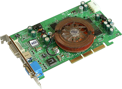
Model: Volari V8 Ultra
Date Released: 2004
Interface: AGP
Shader Model: 2.0
DirectX: 9
Manufacturing Process: 0.13 micron
Core Clockspeed: 300MHz
Memory Clockspeed: 300MHz
Memory Bus: 128-bit
Transistors: 80 million
(Image Credit: hardwareanalysis.com)
Model: Volari V8 Ultra
Date Released: 2004
Interface: AGP
Shader Model: 2.0
DirectX: 9
Manufacturing Process: 0.13 micron
Core Clockspeed: 350MHz
Memory Clockspeed: 350MHz
Memory Bus: 128-bit
Transistors: 80 million
XGI / Trident XG41
While the XG40 chipset targeted (unsuccessfully) the high end graphics market, the XG41 concentrated on the mainstream crowd. It did this via the Volari V5 Ultra, which also came in a dual-GPU Duo package, and cutting the number of rendering pipelines in half from 16 down to 8. Clockspeeds and memory bandwidth remained the same as the V8 series, but the reduced pipelines meant a significantly lower pixel and texture fill rates. As such, benchmarks weren't too impressive.
(Image Credit: pcstats.com)
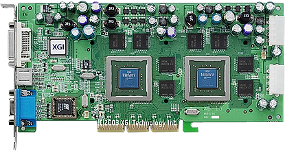
Model: Volari V5
Date Released: 2004
Interface: AGP
Shader Model: 2.0
DirectX: 9
Manufacturing Process: 0.13 micron
Core Clockspeed: 350MHz
Memory Clockspeed: 350MHz
Memory Bus: 128-bit
Transistors: 80 million
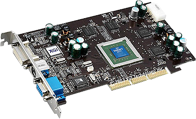
(Image Credit: madboxpc.com)
Model: Volari V5 Ultra
Date Released: 2004
Interface: AGP
Shader Model: 2.0
DirectX: 9
Manufacturing Process: 0.13 micron
Core Clockspeed: 350MHz
Memory Clockspeed: 450MHz
Memory Bus: 128-bit
Transistors: 80 million (x2)
XGI / Trident XG47
The highest numbered graphics chipset in XGI's short-lived lineup, the XG47 also represented the company's lowest end part. Taking aim at the entry-level sector, the XG47-based Volari 8300 released in 2005 slashed the memory interface down to just 64-bit, making it better suited for home theater setups than for pushing gaming pixels.
But one thing the Volari 8300 boasted that the other Volari videocards didn't was a PCI-E interface. This gave the 8300 added appeal to those who had upgraded, or planned to upgrade, their motherboards and leave AGP behind. Surprisingly current (from a spec-sheet standpoint) still today, the 8300 also brought a DVI port to the table and support for the then upcoming Windows Vista operating system.
Low power consumption, an integrated TrueVideo engine, and an effective de-interlacing scheme made the 8300 a good all-around multimedia card, so long as you didn't expect much out of 3D games.
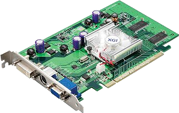
(Image Credit: pc- erfahrung.de)
Model: Volari 8300
Date Released: 2005
Interface: PCI-E
Shader Model: 2.0
DirectX: 9
Manufacturing Process: 0.13 micron
Core Clockspeed: 300MHz
Memory Clockspeed: 300MHz
Memory Bus: 64-bit
Transistors: 90 million
Matrox G550
As time went on, Matrox struggled to remain competitive with Nvidia and 3dfx in terms of gaming performance, and it seemed to almost concede the market with the release of the G550 released in 2001. Rather than take aim at blistering 3D performance, the G550 focused on the budget and mainstream market with slower clockspeeds (125MHz core and 333MHz memory) than the GeForce2 Ultra (200MHz core and 460MHz memory). Morever, Matrox again stayed with a 64-bit memory bus, a clear signal that hardcore gamers need not apply.
On the productivity front, the G550 held a bit more appeal, thanks in large part to its DualHead technology. End users could take advantage of two different monitors running separate resolutions, something neither ATI's HydraVision nor Nvidia's TwinView technology could do, and it worked under Windows 2000.
Matrox also introduced a new Head Casting engine, which was "designed specifically to accelerate the 3D rendering of high-resolution human facial animations over the internet," paving the way for photo-realistic 3D talking heads without hogging bandwidth.
Fun Fact: The Millennium G550 PCI-E was the world's first PCI Express x1 videocard.
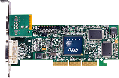
(Image Credit: Matrox)
Model: G550
Date Released: 2005
Interface: AGP/PCI-E
Shader Model: N/A
DirectX: 6
Manufacturing Process: 0.18 micron
Core Clockspeed: 125MHz
Memory Clockspeed: 166MHz
Memory Bus: 64-bit
ATI Radeon R520
ATI had come a long way since the days of 3D Rage, and the biggest shift was yet to come. ATI's engineers had gone back to the drawing board, and what they came up with was the R520, a completely new architecture that was unlike anything that had been done before. Serving as the backbone for the new design was what ATI called an "Ultra-Threading Dispatch Processor." Like a foreman, the UTDP was responsible for telling its workers what to do, and when to do it. In this case, the 'workers' were four groups of four pixel shaders, 16 in all. This technique proved highly efficient and allowed ATI to get away with utilizing less pixel shaders than the 24 employed by the competition.
The R520 also had a redesigned memory controller. The new controller used a weighting system responsible for prioritizing which clients needed access to data the quickest.
Several other advancements had been made, most of which focused on efficiency. Image quality was better, full High Dynamic Range (HDR) lighting was implemented for the first time, and better DVD decoding were among the improvements that had been made.
Fun Fact: At the extreme high end, some graphics partners implemented a self-contained water-cooling assembly on the X1950 XTX.
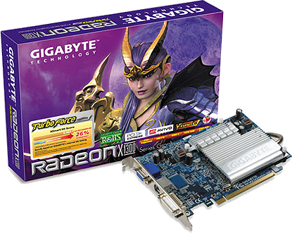
(Image Credit: Gigabyte)
Model: Radeon X1300
Date Released: 2005
Interface: AGP/PCI-E
Shader Model: 3.0
DirectX: 9
Manufacturing Process: 90nm
Core Clockspeed: 450MHz
Memory Clockspeed: 533MHz
Memory Bus: 128-bit (64-bit PCI)
Transistors: 105 million
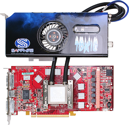
(Image Credit: computershopper.com)
Model: Radeon X1950 XTX
Date Released: 2006
Interface: PCI-E
Shader Model: 3.0
DirectX: 9
Manufacturing Process: 90nm
Core Clockspeed: 650MHz
Memory Clockspeed: 1000MHz
Memory Bus: 256-bit
Transistors: 384 million
Next, the race to a TFLOP continues with only two dominant contenders
Paul has been playing PC games and raking his knuckles on computer hardware since the Commodore 64. He does not have any tattoos, but thinks it would be cool to get one that reads LOAD"*",8,1. In his off time, he rides motorcycles and wrestles alligators (only one of those is true).
 Join The Club


