From Voodoo to GeForce: The Awesome History of 3D Graphics
Matrox G400/G450
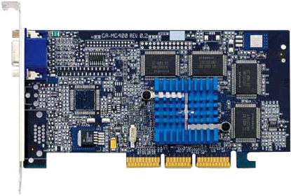
Moving up the Matrox line, the G400 picked up where the G200 left off and sported several improvements. What didn't change was the 0.25-micron manufacturing process, and Matrox ported its DualBus architecture to the new chipset, but everything else about the G400 was either bigger or better. The 64-bit bus had been upgraded to 128-bit, a second pixel pipeline and texture unit was added, core clockspeed was increased to 125MHz, and both the texture and pixel fill rates went up from 85 MP/s and MT/s to 250 MP/s and MT/s, respectively.
The G400 also introduced a feature called DualHead. This allowed end users to extend their desktops across two monitors, a capability that most power users take for granted today, but one that gave Matrox a marketing bullet its competition didn't have.
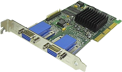
Following a familiar pattern, Matrox in 2000 released the G450 chipset, which introduced a shrunken die (0.18- micron) and integrated the G400's second RAMDAC onto the chip. Matrox also decided to cut the memory bus in half to 64-bit, hoping the switch to DDR memory would make up for the reduced bandwidth. It didn't, and as a result, the G400 proved a better gaming card in most situations.
Fun Fact: A special version of the G400 known as the Marvel G400-TV added a TV tuner, along with hardware MPEG video capture and editing capabilities.
(Image Credit: SharkyExtreme.com)
Model: G400
Date Released: 1999
Interface: AGP
Shader Model: N/A
DirectX: 6
Manufacturing Process: 0.25 micron
Core Clockspeed: 125MHz
Memory Clockspeed: 166MHz
Memory Bus: 128-bit
(Image Credit: emertx-info.com)
Keep up to date with the most important stories and the best deals, as picked by the PC Gamer team.
Model: G450
Date Released: 2000
Interface: AGP/PCI
Shader Model: N/A
DirectX: 6
Manufacturing Process: 0.18 micron
Core Clockspeed: 125MHz
Memory Clockspeed: 166MHz
Memory Bus: 64-bit
3dfx VSA-100 Series
By this time, 3dfx's storied run was coming to an end. The competition had caught up with, and surpassed, the Voodoo series, with Nvidia's GeForce 256 starting to steal the limelight. In March of 2000, 3dfx acquired chip maker GigaPixel Corp. for around $186 million, a move that would prove fatal. Shortly after the acquistion, 3dfx released its first Voodoo Scalable Architecture (VSA) videocards (Voodoo4 and Voodoo5), which were designed to support multiple chip configurations.
At the lower end, the Voodoo4 4500 came configured with a single VSA-100 chip, up to a 367 MPixel fill rate, and 32MB of memory. Higher up on the performance ladder, the Voodoo5 5000 came with two VSA-100 chips, up to a 773 MPixel fill rate, and a 64MB buffer. 3dfx also planned to release a Voodoo5 6000, but a manufacturing defect kept the card from ever making it to market.
These would be last cards 3dfx would ever release due to piling debt and increasingly impatient creditors. In December 2000, rival Nvidia announced it had signed a definitive agreement to acquire 3dfx's intellectual graphics assets.
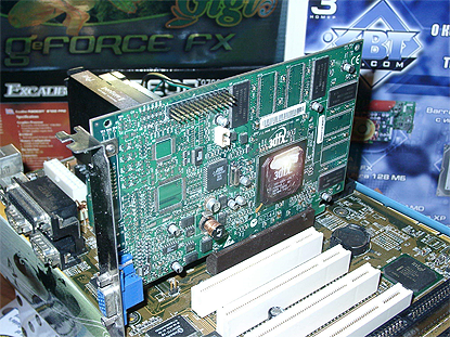
(Image Credit: ixbt.com)
Model: Voodoo4 4500
Date Released: 2000
Interface: AGP/PCI
Shader Model: N/A
DirectX: 6
Manufacturing Process: 0.22 micron
Core Clockspeed: 183MHz
Memory Clockspeed: 183MHz
Memory Bus: 128- bit
Transistors: 14 million
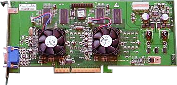
(Image Credit: techreport.com)
Model: Voodoo5 5500
Date Released: 2000
Interface: AGP/PCI
Shader Model: N/A
DirectX: 6
Manufacturing Process: 0.22 micron
Core Clockspeed: 166MHz
Memory Clockspeed: 166MHz
Memory Bus: 128-bit
Transistors: 14 million (x2)
Nvidia GeForce 2 (NV11, NV15, NV16)
How does 1.6 billion texels per second sound? In the year 2000, such a feat sounded pretty damn impressive, considering Nvidia's previous generation product pushed out over three times less than that. It wasn't that the GeForce 2 was a wholly different architecture, but adding a second texture map unit (TMU) to each of its 4 pixel pipelines helped boost performance, as did a much faster core clockspeed. An early form of pixel shaders, called Nvidia Shading Rasterizer (NSR) was also introduced.
The GeForce 2 ran circles around the GeForce 256 in some games, however ATI and 3dfx offered stiff competition with a more efficient handling of memory bandwidth and RAM controllers.
From a sales perspective, the somewhat crippled GeForce 2 MX proved immensely popular for its low price and serviceable 3D performance. The MX had two less pixel pipelines and half the memory bandwidth, but retained hardware T&L. Eventually, the MX variant would provide the basis for Nvidia's integrated motherboard graphics.
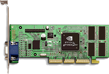
(Image Credit: trustedreviews.com )
Model: GeForce 2 MX
Date Released: 2000
Interface: AGP
Shader Model: N/A
DirectX: 7
Manufacturing Process: 0.08 micron
Core Clockspeed: 176MHz
Memory Clockspeed: 166MHz
Memory Bus: 128-bit
Transistors: 20 million
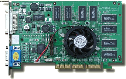
(Image Credit: tomshardware.com )
Model: GeForce 2 GTS
Date Released: 2000
Interface: AGP
Shader Model: N/A
DirectX: 7
Manufacturing Process: 0.22 micron
Core Clockspeed: 200MHz
Memory Clockspeed: 333MHz
Memory Bus: 128-bit
Transistors: 25 million
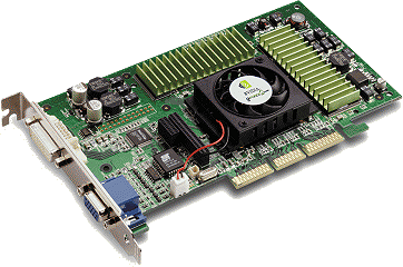
(Image Credit: nvnews.net)
Model: GeForce 2 Ultra
Date Released: 2000
Interface: AGP
Shader Model: N/A
DirectX: 7
Manufacturing Process: 0.22 micron
Core Clockspeed: 260MHz
Memory Clockspeed: 460MHz
Memory Bus: 128-bit
Transistors: 25 million
ATI Radeon R100
Originally intended as the next generation of Rage cards, the R100 ditched its Rage 6 code-name and instead kicked off the long-standing Radeon line that remains today and into the foreseeable future. This first generation Radeon was released in 2000 with 32MB or 64MB of DDR memory. Later that year, ATI would release a pair of Radeons with SDR memory, although these would be slower and in the case of the Radeon LE, also severely gimped. Still, the LE proved popular among overclockers, who made up for the card's shortcomings by ramping up its core and memory clockspeeds.
ATI would build several R100-based videcoards throughout the architecture's lifetime, including another All-in-Wonder version, the AIW 7500. Save for the Radeon 7000 VE, all of these cards boasted a 128-bit memory bus. Stock core clockspeed ranged anywhere from 167MHz to 290MHz, and each iteration supported hardware T&L, save again for the 7000 VE.
Fun Fact: After the Radeon 8500 came to market, ATI went back and applied the Radeon 7200 nomenclature to all R100-based cards.
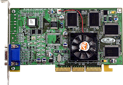
(Image Credit: ixbt.com)
Model: Radeon SDR (7200)
Date Released: 2000
Interface: AGP/PCI
Shader Model: N/A
DirectX: 7
Manufacturing Process: 0.18 micron
Core Clockspeed: 167-183MHz
Memory Clockspeed: 166MHz
Memory Bus: 128-bit
Transistors: 30 million
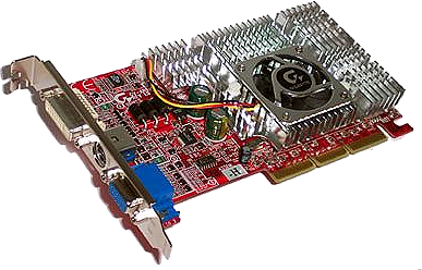
(Image Credit: techtree.com)
Model: Radeon 7500
Date Released: 2001
Interface: AGP/PCI
Shader Model: N/A
DirectX: 7
Manufacturing Process: 0.18 micron
Core Clockspeed: 290MHz
Memory Clockspeed: 230MHz
Memory Bus: 128-bit
Transistors: 30 million
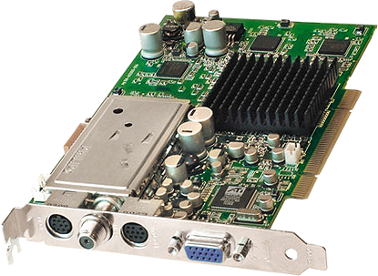
(Image Credit: rage3d.com)
Model: Radeon 7500 All-in-Wonder
Date Released: 2001
Interface: AGP/PCI
Shader Model: N/A
DirectX: 7
Manufacturing Process: 0.18 micron
Core Clockspeed: 167-183MHz
Memory Clockspeed: 167-183MHz
Memory Bus: 128-bit
Transistors: 30 million
Next, programmable shaders arrive and change graphics forever
Paul has been playing PC games and raking his knuckles on computer hardware since the Commodore 64. He does not have any tattoos, but thinks it would be cool to get one that reads LOAD"*",8,1. In his off time, he rides motorcycles and wrestles alligators (only one of those is true).

