From Voodoo to GeForce: The Awesome History of 3D Graphics
Nvidia NV5
Now entering its fifth generation of videocards, Nvidia took its NV4 architecture and moved to a smaller 0.25-micron manufacturing process. This allowed Nvidia to push clockspeeds up to almost 70 percent faster than it had before. The maximum amount of onboard memory was again doubled, this time to 32MB, and AGP 4X support was also added to NV5.
Nvidia would attack all three market segments -- entry-level, mid-range, and high-end -- with the NV5-based TNT2, all of which were Directx6-capable videocards. At the lower end, however, Nvidia would slice the memory bus in half from 128-bit to 64-bit. This would still run faster than the older NV4-based TNT, making them very good value cards.
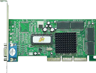
(Image Credit: eletech.com)
Model: Riva TNT 2 Vanta
Date Released: 1999
Interface: AGP/PCI
Shader Model: N/A
DirectX: 6
Manufacturing Process: 0.25 micron
Core Clockspeed: 100MHz
Memory Clockspeed: 125MHz
Memory Bus: 64-bit
Transistors: 15 million
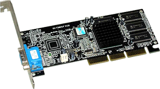
(Image Credit: Photobucket mypapit)
Model: Riva TNT 2
Date Released: 1999
PC Gamer Newsletter
Sign up to get the best content of the week, and great gaming deals, as picked by the editors.
Interface: AGP/PCI
Shader Model: N/A
DirectX: 6
Manufacturing Process: 0.25 micron
Core Clockspeed: 125MHz
Memory Clockspeed: 150MHz
Memory Bus: 128-bit
Transistors: 15 million

(Image Credit: Nvidia)
Model: Riva TNT 2 Pro
Date Released: 1999
Interface: AGP/PCI
Shader Model: N/A
DirectX: 6
Manufacturing Process: 0.22 micron
Core Clockspeed: 143MHz
Memory Clockspeed: 166MHz
Memory Bus: 128-bit
Transistors: 15 million
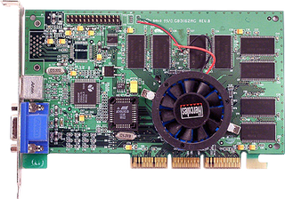
(Image Credit: ixbt.com)
Model: Riva TNT 2 Ultra
Date Released: 1999
Interface: AGP/PCI
Shader Model: N/A
DirectX: 6
Manufacturing Process: 0.25 micron
Core Clockspeed: 150MHz
Memory Clockspeed: 183MHz
Memory Bus: 128-bit
Transistors: 15 million
PowerVR Series 2
A year and a half late to market, the Neon 250 debuted in 1999 running at 125MHz and touting 32MB of high speed SDRAM. and a 250MHz RAMDAC. The Neon 250 could process up to 4 million polygons per second, offered advanced texturing (Bilinear, trilinear, anisotropic, and bump mapping), D3D and OpenGL blend modes, and a host of other specs.
But what really made the Neon 250 stand out was it's unique (at the time) approach to 3D computing. Rather than display images by processing polygons one at a time -- through the CPU and the GPU -- the Neon 250 took a 'tile-based' approach. Each 3D scene would be broken up into separate small tiles and independently processed before being sent through the GPU. Hidden surfaces wouldn't be processed, saving Z-bugger memory and memory bandwidth, while also requiring less graphics processing power.
A great card on its own merit, the Neon 250 would have been a bigger success had PowerVR been able to ship it on time. However, the delays proved costly in terms of going toe-to-toe with the competition, who had a leg up on the Neon 250 by the time it actually came to market.
Fun Fact: Old school console gamers will remember PowerVR as the company who supplied the processor for Sega's Dreamcast console. And in fact PowerVR's VR2-based Neon 250 was essentially the much anticipated PC version of the same chip.
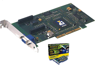
(Image Credit: tilebase.de)
Model: Neon 250
Date Released: 1999
Interface: AGP/PCI
Shader Model: N/A
DirectX: 6
Manufacturing Process: 0.25 micron
Core Clockspeed: 125MHz
Memory Clockspeed: 125MHz
Memory Bus: 128-bit
Trident TVGA and Blade
Pour yourself a cold one if you still own one of the earlier Trident TVGA videocards. First introduced over two decades ago in 1987, Trident's TVGA 8200LX kicked off an extensive line of TVGA videocards that would extend to the 1990s. Can you say ISA?
We can, but we'd rather say Blade, the name of what many consider to be Trident's first real foray into the 3D acceleration on the Windows platform. The first Blade3D card packed 8MB of video memory and came in both PCI and AGP flavors. Later revisions would add faster clockspeeds. The end result was a card that offered playable framerates in Quake 2 and competed well against Intel's i740, but couldn't keep up with Nvidia's Riva TNT or the Matrox G200.
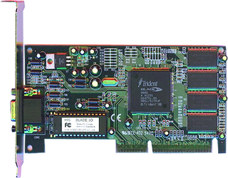
(Image Credit: anime.net)
Blade3D: No Shader Model, no DX support, 0.25 micron AGP, 120MHz core, AGP, 128-bit
Model: Blade3D
Date Released: 1999
Interface: AGP
Shader Model: N/A
DirectX: 6
Manufacturing Process: 0.25 micron
Core Clockspeed: 110MHz
Memory Clockspeed: 120MHz
Memory Bus: 128-bit
3dfx Voodoo3
Codenamed 'Avenger,' the Voodoo3 combined the best 3dfx had to offer up to this point in a single videocard. Like the Banshee, the Avenger sported a single-chip, 2D/3D-capable design, but it also included mutlitexturing support. Other features included a 128-bit GDI accelerator, dual 32-bit pipelines, a 300MHz - 350MHz RAMDAC, up to 16MB of memory, and support for resolutions up to 2046x1536.
There would be several versions of the Voodoo3, both in PCI and AGP form, with the higher model numbers representing faster clockspeeds. In addition, the Voodoo3 3500 TV would add an integrated TV-tuner to the mix capable of real-time MPEG-2 video and audio capture.
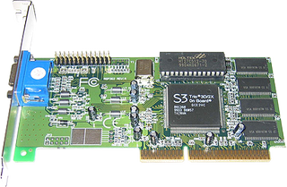
(Image Credit: pacificgeek.com)
Model: Voodoo3 1000
Date Released: 1999
Interface: AGP/PCI
Shader Model: N/A
DirectX: 6
Manufacturing Process: 0.25 micron
Core Clockspeed: 125MHz
Memory Clockspeed: 125MHz
Memory Bus: 128-bit
Transistors: 8.2 million
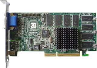
(Image Credit: freewebs.com)
Model: Voodoo3 2000
Date Released: 1999
Interface: AGP/PCI
Shader Model: N/A
DirectX: 6
Manufacturing Process: 0.25 micron
Core Clockspeed: 143MHz
Memory Clockspeed: 143MHz
Memory Bus: 128-bit
Transistors: 8.2 million
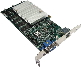
(Image Credit: mateusz.niste.free.fr)
Model: Voodoo3 3000
Date Released: 1999
Interface: AGP/PCI
Shader Model: N/A
DirectX: 6
Manufacturing Process: 0.25 micron
Core Clockspeed: 125MHz
Memory Clockspeed: 125MHz
Memory Bus: 128- bit
Transistors: 8.2 million
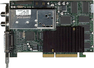
(Image Credit: rashly3dfx.com)
Model: Voodoo3 3500 TV
Date Released: 1999
Interface: AGP/PCI
Shader Model: N/A
DirectX: 6
Manufacturing Process: 0.25 micron
Core Clockspeed: 183MHz
Memory Clockspeed: 183MHz
Memory Bus: 128-bit
Transistors: 8.2 million
Nvidia GeForce 256 (NV10)
Today's Nvidia-branded desktop cards carry the GeForce nomenclature, a naming scheme that first began a decade earlier. Also known as NV10, the GeForce 256 architecture came into being in 1999 and offered significant speed gains over its predecessor, almost twice as fast in some cases, and allowed Nvidia to snatch the performance crown from 3dfx in dramatic fashion.
The GeForce 256's quad-pixel rendering pipeline could pump 480 M/texels, which was about 100-166M more than other videocards on the market. It also came equipped with hardware T&L and a feature called cube environment mapping for creating real-time reflections.
It's worth noting at this point that Nvidia's decision to remain a fabless manufacturer was really starting to pay off. Third party add-in board (AIB) partners flooded the market with Nvidia silicon, allowing the chip maker to make a steady profit selling its chips regardless of what price point(s) each board partner sold their cards.
Fun Fact: Nvidia hailed the GeForce 256 as "the world's first GPU," a claim made possible by being the first to integrate a geometry transform engine, a dynamic lighting engine, a 4-pixel rendering pipeline, and DirectX 7 features onto the graphics chip.
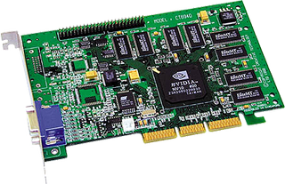
(Image Credit: SharkyExtreme)
Model: GeForce 256
Date Released: 1999
Interface: AGP
Shader Model: N/A
DirectX: 7
Manufacturing Process: 0.22 micron
Core Clockspeed: 120MHz
Memory Clockspeed: 166MHz
Memory Bus: 128-bit
Transistors: 23 million
Next, did users bite with Matrox's innovative DualHead feature?
Paul has been playing PC games and raking his knuckles on computer hardware since the Commodore 64. He does not have any tattoos, but thinks it would be cool to get one that reads LOAD"*",8,1. In his off time, he rides motorcycles and wrestles alligators (only one of those is true).

